要約
Understand the value of a µP supervisor to ensure proper system operation during power-up, power-down, and brownout situations (undervoltage monitoring). In addition, provides information about overvoltage and windowed monitoring. Describes additional features such as manual reset, watchdog timer, battery backup, and chip enable gating. Discusses the need for multi-voltage monitoring.
Microprocessor-supervisory circuits have been around for so many years that they are often taken for granted. Not so the modern integrated-circuit versions, which range from simple three-terminal reset chips to complex multifunction devices. Maxim alone offers nearly 100 part numbers, each with variations that total thousands of products. By understanding these products and their basic functions, board-level designers can handle the simplest and most complex of applications.
The most fundamental function of a microprocessor (µP) supervisor is that of "power-on-reset" (POR). Otherwise well-behaved µP-based systems can exhibit problems during power-up or when the supply voltage sags temporarily (brownout). For many years, the partial solution to this problem has been the addition of a resistor, a capacitor, and a diode to the µP's Active-low RESET line (Figure 1).
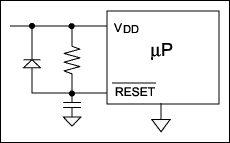
Figure 1. This crude supervisory circuit is only a partial solution to the problem of monitoring VDD.
The added RC causes Active-low RESET to be held low after the supply voltage starts to come up. If the voltage rises quickly enough, Active-low RESET will be sufficiently low to hold the µP in reset, allowing its circuitry to settle down before normal operation is resumed. When the power supply turns off and drops to zero, the diode ensures a prompt high-to-low transition for Active-low RESET as well.
This method works reasonably well for power-up as long as the power supply rises quickly with respect to the RC time constant. The circuit's job is to protect the µP from less-than-perfect power-ups, but it relies on the supply voltage to rise quickly enough for that purpose. It is also unreliable in resetting the µP during a brownout. To achieve reset for that condition, the supply voltage must drop to a level of VIL minus one diode drop. Long before it reaches this level, however, the supply voltage is well below its minimum spec.
To handle this situation, microprocessor vendors often recommend a circuit comparable to that in Figure 2. It forces a reset when the power supply drops, but voltage accuracy is limited to that of the zener diode combined with errors associated with the transistor characteristics.
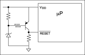
Figure 2. This circuit adds brownout capability to the VDD monitor in Figure 1, but it offers limited accuracy and utility.
A timeout function can be grafted onto this circuit with the addition of a capacitor and a diode. The resulting circuit has seven components, and it still has a problem with accuracy and with slow-rising supply voltages.
How Accurate Is Accurate Enough?
Consider a common example in which the processor operates on a nominal 5V supply and is specified to operate as low as 4.5V. The reset circuit should hold reset for all voltages below 4.5V, and its minimum threshold must therefore be 4.5V. What, then, should be the upper limit for the spread of reset thresholds over temperature and from unit to unit? You can specify the power supply at 5V ±0% if you want to get in trouble with the power supply designers, but a more likely range is 4.75V to 5.25V. You should therefore guarantee the threshold between 4.5V and 4.75V; i.e., 4.63V ±2.7%.
A zener diode can regulate the threshold voltage, but the accuracy of a typical zener is ±5% to ±10%. For premium prices you can specify tighter tolerance (to ±1%), but only for room temperature and a specific current. All zeners exhibit a significant variation of voltage with current, and the typical temperature coefficient (TC) is several mV/°C. TC alone can cause several hundred millivolts of change over the range 0°C to 70°C. Zener-based reset circuits are inadequate to guarantee a proper reset on startup and during a brownout. To make matters worse, even low-current zeners require 100µA to achieve regulation, which is a considerable load in battery-powered systems.
How Should an Ideal Reset Circuit Operate?
We've established that the reset circuit's voltage tolerance should not exceed ±2.7% over temperature. But without a proper delay in terminating the reset pulse, the circuit is subject to malfunction under two conditions: a slow-rising supply voltage as mentioned earlier or a supply voltage that exhibits noise or nonmonotonic behavior during startup or recovery from brownout conditions. If the monitored supply voltage sits right at the reset circuit threshold, noise will tend to trigger, untrigger, and retrigger the circuit repeatedly, causing the µP's Active-low RESET input to oscillate.
Hysteresis can cure this problem, and the market offers several families of voltage-detector products that attempt to solve the dilemma that way. Unfortunately, hysteresis narrows the threshold's allowable voltage tolerance. We had 250mV (4.75V Ð 5.0V) to play with in the above example. If you add 100mV of hysteresis, the minimum threshold for a rising voltage becomes 100mV higher than before, i.e., 4.6V rather than 4.5V. This shift is necessary to guarantee that the threshold for a falling voltage (during brownouts) will be no lower than 4.5V. Thus, to ensure both thresholds between 4.5 and 4.75V, the upper one must be 4.67V ±1.6%.
Common voltage detectors of this type, such as the Ricoh Rx5VL/Rx5VT and Seiko S-807, have 25°C threshold accuracy of ±2.5% and ±2.4%. Actual devices operate beyond 25°C, but these products specify only typical temperature coefficients of 100ppm/°C and 120ppm/°C. These TCs result in threshold tolerances of ±2.85% and ±2.82%, respectively, over the 0° to 70°C range.
The Seiko S-808 family represents the more recent precision parts of this type. They specify ±2% accuracy at 25°C and a maximum temperature coefficient of 350ppm/°C. Over the 0°C to 70°C range, this maximum temperature coefficient corresponds to a variation of 350e-6 x 70 = 0.0245, or 2.45%. Our worst-case accuracy is therefore ±3.225%. If we assume a worst-case part will not exhibit the maximum temperature coefficient over temperature but rather (on average) about half the maximum, then the resulting maximum variation (±2.6125%) is just good enough for the above example.
We haven't yet considered hysteresis. The above analysis shows that the rising-edge threshold fits our specification. The falling-edge threshold will be lower, however. Hysteresis for all these detectors is 5% typical and 7% or 8% maximum. The rising-edge threshold in our example is within the required range (4.5V to 4.75V), but the falling-edge threshold can be as low as 4.13V. That is, we cannot guarantee brownout detection until the supply voltage is almost 0.4V out of spec!
Electronic Procrastination Is the Answer
To prevent oscillatory behavior at the detection threshold without resorting to excessive hysteresis, we must delay the trailing edge of the reset pulse. As in the RC circuit described above, the reset pulse must hold for an interval after the supply voltage crosses the detector's threshold. This interval is called "delay time" or the "reset active-timeout period." Unlike the RC circuit delay, however, this one triggers when supply voltage crosses a precisely trimmed threshold in the detector. The delay should also be retriggerable to prevent oscillation in the µP's reset signal. When a slowly rising supply voltage causes multiple trigger events at the detector threshold, each event should re-start the timeout.
Devices offering this basic function have been around for a long time, and in recent years have become available in the tiny, three-terminal SOT23 package. The first SOT23 device (MAX809) has become a much-copied industry standard. The generic 809 is available with several factory-trimmed reset thresholds, and it offers a guaranteed accuracy of ±2.6% over the -40°C to +85°C range. The 809 also guarantees a minimum active-timeout reset period of 140ms. It provides all the features described above and is much simpler than discrete-component approaches. Figure 3 illustrates the simplicity of an 809 circuit.
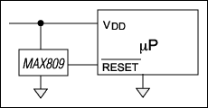
Figure 3. A three-terminal supervisory IC combines voltage monitoring (startup and brownout) with reset-delay capability.
The MAX809 draws as much as 60µA. Some recent clones of this part, including IMP's IMP809 and ETC's ETC809, feature maximum supply currents in the 15µA to 20µA range. The new MAX6326 and MAX6346 families, however, provide the same functionality with much lower supply currents. They draw 1µA maximum (0.5µA typical) for threshold voltages below 3.2V and 1.75µA maximum (1µA typical) for higher threshold voltages.
When Power-Supply Monitoring Is Not Enough
Three-terminal supervisors provide the primary supervisory function, but many applications require more of the supervisor. A basic function often needed is pushbutton or manual-reset input. This capability lets you initiate resets with a momentary pushbutton switch. It can also gate multiple binary signals or another reset to the µP's reset input. This input is debounced with the same delay function used in the power-supply monitor. The enhanced supervisor requires a fourth pin, which is provided by the SOT-143 (a four-pin SOT-23). Most manufacturers of the three-terminal devices mentioned above also make four-terminal devices that include this feature.
Most of the earlier SOT devices are available in five or so standard threshold voltages. However, two of the four-terminal devices from Maxim (MAX6314 and MAX6315) represent the first in a growing line of supervisors that make available a wide range of custom thresholds and reset timeouts. The most common combinations are available as standard products, but the engineer can also specify threshold voltages from 2.5V to 5.0V in 100mV increments and minimum reset-delay times of 1ms, 20ms, 140ms, or 1.12s.
Woof!
Another common requirement for microprocessor-based systems is the watchdog timer (WDT). WDTs provide protection against rogue software and other aberrations that cause software execution to "run off into the weeds." The WDT is simply a restartable timer whose output (Active-low WDO) changes state on timeout, resetting the µP or generating an interrupt. To prevent the WDT from timing out, you connect an I/O line from the µP to the WDT input (WDI). Then, software must produce transitions on this line that repeatedly restart the watchdog before timeout. Otherwise, the WDO triggers an interrupt or reset.
But My Microprocessor Has a Watchdog Function
Many µPs have internal watchdog timers, but many of these WDTs do not provide complete protection. Often the WDT can be disabled as well as enabled by software. If software can disable the WDT, then the WDT cannot completely protect the system from software. To remove this liability, you need an external hardware watchdog timer that cannot be disabled by software.
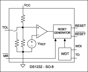
Many parts have this function, including the ubiquitous DS1232 from Dallas Semiconductor; it is one of the most duplicated supervisory circuits on the market (Figure 4a). This part provides the same functionality as four-terminal devices, plus a WDT that can be programmed via its TD pin for any of three different periods. Using the TOL pin, you can also set the threshold to one of two factory-set voltages. The '1232 also has complementary reset outputs. The original version was available only in eight-pin DIPs and the 16-pin wide-SO package. Newer versions are available in the eight-pin SO.
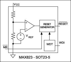
Most applications do not need the '1232's programmability or complementary outputs. Eliminating these features drops the pin count to five, allowing the remaining functionality to be implemented in a five-pin version of the SOT23. The first such parts available in a five-pin SOT23 are the MAX823 and MAX824 (Figure 4b). As with the '1232, their WDT output is internally gated with the power monitor output to provide a single Active-low RESET output. The MAX823 has an active-low Active-low RESET, and the MAX824 has an active-high RESET.
|
|
|
|
Figure 4a. |
Figure 4b. |
Figure 4. These popular supervisory ICs include watchdog timers and a manual-reset input.
As with the three- and four-terminal devices, these first five-pin SOT devices have spawned a family of parts that provide greater variation and flexibility for the designer. MAX6316 through MAX6322 devices, for example, provide a variety of feature combinations and output structures in the SOT23-5. Available versions of these products offer reset thresholds in 100mV increments between 2.5V and 5.0V, four different minimum reset timeouts (1ms, 20ms, 140ms, or 1.12s), and four different minimum WDT timeout periods (4.3ms, 71ms, 1.12s, or 17.9s).
Monitoring Multiple Voltages with a Single Chip
Many systems require multiple supply voltages for operation. These voltages can be monitored with multiple devices, but most designers prefer a single device to monitor two or more voltages. The Dallas DS1834, for instance, monitors a 5V supply and a 3V or 3.3V supply.
Systems that include both analog and digital circuitry often require that you monitor a digital supply voltage along with positive and negative analog supply voltages simultaneously. A MAX6304, MAX6307, or MAX6310 (available in SOT packages), plus four external resistors can do this job. The ICs differ only in the structure of their reset outputs: low-true open-drain, low-true push-pull, or high-true push-pull. They monitor voltages at the VCC pin using factory-preset reset thresholds that range from 2.5V to 5.0V in 100mV steps. Each device includes externally set undervoltage and overvoltage comparators whose thresholds are set by external voltage dividers. The under- and overvoltage inputs for these two comparators can implement a windowed reset function that gives warning (by generating a reset) when a particular voltage is either too high or too low.
Alternatively, you can use the overvoltage input as an undervoltage detector for a negative voltage. Combining this function with the preset and configurable undervoltage detector enables the chip to monitor a logic voltage such as 5V along with positive and negative analog voltages such as ±12V (Figure 5). The device shown has a low-true push-pull reset output (6310 base number), a nominal 4.63V preset threshold ('46' suffix), and a nominal 200ms reset timeout (D3 suffix). The external resistors shown generate resets when the analog voltages are less than ±10V.
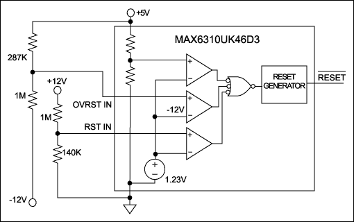
Figure 5. Internal comparators implement undervoltage/overvoltage warnings and windowed-reset functions.
To ensure the continuity of SRAM contents and other critical functions when supply voltage is lost, many of the older supervisory circuits are able (concurrently with reset) to switch the power source applied to such subsystems from the system supply to a backup battery. The need for this battery-backup switchover is in decline with the advent of flash memory, but it still exists in many systems. Most of the older supervisor chips have internal switches for the battery and the system supply, and for larger loads they can also switch the system supply by driving an external transistor.
A companion feature to battery-backup switchover is chip-enable write protection or chip-enable gating (Active-low CE gating). The Active-low CE line from µP or address-decode logic, which normally goes to the SRAM, is routed instead through the supervisory chip to the SRAM. This signal normally passes through the chip unaltered. During reset, however, the supervisory chip forces Active-low CE high, disabling access to the memory and thereby protecting the SRAM contents from errant writes by a µP that has temporarily lost its mind.
Most recent supervisory chips are relatively simple devices that reside in small packages such as the SOT, but some offer additional features. The MAX818, for example, provides basic power-monitoring and watchdog capability, along with battery-backup switchover and CE gating in an eight-pin µMAX package (Figure 6). The battery-backup switchover circuit in this part also provides a "battery freshness seal" that prevents the discharge of batteries installed in products before shipment.
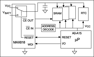
Figure 6. This supervisory device includes a watchdog timer, battery-backup switchover, and chip-enable gating, along with basic supply-voltage monitoring.
The freshness seal is enabled during production of the product: With the battery installed, the test equipment forces the Active-low CE OUT line to ground, applies VCC, and then removes VCC after the reset timeout period has expired. The internal battery-backup circuit keeps the battery and the load disconnected even when the supervisory chip is powered off. The chip then returns to normal operation the next time VCC is applied (without externally holding Active-low CE OUT low).
Another feature offered in more complex devices is low-line output. This binary output is triggered by an internal comparator that monitors the supply voltage with a threshold slightly above the reset threshold. By monitoring this pin via an interrupt, the µP gets an advance warning of any impending reset due to a voltage sag.
Some devices provide an internal "power-fail" comparator, with one input connected to the internal reference and the other input (and output) uncommitted. This arrangement allows the designer to detect any desired voltage level using an external voltage divider. It is often used to detect raw voltage from a battery or line-derived source applied to the VCC regulator. The power-fail output informs the µP when the input voltage is getting close to the minimum allowed for proper regulation. This early warning can allow the system to perform an orderly shutdown before the power fails. Examples of such complex, multifunction supervisory circuits include the DS1236, the MAX793, and the MAX807.
The requirements of certain complex, mission-critical applications, however, are beyond the capability of any single chip, including these multifunction supervisors. A good example is the high-end multi-axis motion controllers from Motion Engineering Inc. (Santa Barbara, CA). These systems (the XMP family) implement a unique, comprehensive protection scheme using a combination of standard supervisors and some minimal external logic (Figure 7). The initial members of this family (a PCI version and a Compact PCI (CPCI) version) provide 150+ MFLOPS of DSP power and control up to 16 axes; i.e., 16 motors in close synchronization.

Figure 7. Multiple ICs provide supervisory protection for a sophisticated mission-critical system.
Because the de-facto standard interface between a controller and a motor drive is a ±10V signal, the XMP generates ±15V supply voltages with on-board DC-DC converters to power the output stages. It utilizes these voltages as well as the ±12V, +5V, and +3.3V that are standard with CPCI specifications. For the PCI version of the motion controller, 3.3V is derived from 5V using another DC-DC converter. Because the analog outputs control motor speed (or torque) directly, they reset to zero during a fault condition. The system monitors all supply voltages, and it shuts down the analog outputs if any supply voltage goes out of spec.
Similarly, the hardware employs a watchdog timer (WDT) to guard itself, the motors, and the motor loads against the effect of software problems. The WDT's short timeout (4ms) catches error conditions before damage is done. At boot-up, the WDT must hold off until the host computer and XMP power up and become synchronized. Then, the WDT becomes enabled in such a fashion that the software cannot disable it again without a full reset of the DSP.
The host computer or an external signal can also trigger a hard reset, one that causes a complete reboot, placing the board in the same state as that following an initial power-up. The WDT triggers soft resets only, which reset the analog outputs and cause the FPGAs to reset their I/O without reloading their configurations. The soft reset condition is latched until the host decides what to do. All other sources cause hard resets.
One MAX6307 monitors the ±15V supplies; another monitors the ±12V supplies. As described above, the overvoltage inputs serve as undervoltage detectors for the negative supply voltages. The open-drain reset outputs are wire-ORed and gated with a reset generated by the host, which writes a specific value through the PCI interface to a CPLD register. The result is applied to the Manual Reset (/MR\) input of a MAX6315, and an External Reset input is applied to the /MR\ input of another MAX6315. One '6315 (factory set for 4.63V) monitors the 5V supply, and the other (factory set for 2.93V) monitors the 3.3V supply. Their wire-ORed outputs produce hard resets that cause the entire board to return to the power-up state.
A MAX6303 in a µMAX package is used for the watchdog timer. This device uses two external capacitors to set independent timeout periods for the watchdog and reset functions. The watchdog period is multiplied by 1X or 500X according to the state of the WDS digital input. The combination of an external WDT capacitor and the WDS pin provides WDT periods from 100µs to many minutes. The MAX6303 also has an undervoltage detector (not used) that is set with two external resistors.
Driving the MAX6303 WDS pin high and floating its WDI input disables its WDT. Employing this feature and two flags in the DSP circuitry in a CPLD on the XMP disables the MAX6303's WDT after a hard reset. The first flag serves as the WDT STROBE; the second as the WDT /ENABLE\ (low true). The STROBE signal goes through a three-state buffer in the CPLD before being applied to WDI. The ENABLE signal is registered by a flip-flop on the CPLD, and the flip-flop output controls the strobe's three-state buffer.
This flip-flop and similar CPLD circuitry in the path of the STROBE signal ensures that both signals come up in a high state, thus disabling the WDT. Once the DSP boots properly, it sets the ENABLE flag low. This action clears the WDS flip-flop to zero, which allows the STROBE signal to propagate out of the CPLD to the WDT input. This transition enables the WDT. The flip-flop is configured such that the WDS input cannot go high again without a full reset of the DSP. To avoid a soft reset, the DSP must now service the WDT every 4ms.
Timeout of the WDT asynchronously latches its reset output in the CPLD, which in turn clears the host interface registers residing in the CPLD. This action flags the host that a soft reset has occurred. The latched reset exits the CPLD to soft-reset the FPGA, and is also gated with the hard reset (MAX6315 output) to disable (zero) the analog outputs. A 74x08 gate in a SOT package, which operates down to very low voltages, ensures that the reset remains valid when the 5V supply sags. Because the analog-control outputs have been disabled, the host can now decide at its leisure what to do. It can reboot the DSP through the PCI interface and remove the soft reset by clearing the latch when the DSP is ready. Alternatively, it can reboot the entire system.
Using three standard supervisory products, a common SOT23-packaged gate, and minimal CPLD resources, MEI has implemented very sophisticated protection. The circuit comprises five SOT packages, eight small resistors, two small capacitors, and a single eight-pin µMax package half the size of a SO-eight package. The total board space required is roughly the same as that occupied by a standard 16-pin SO and an eight-pin SO package.
Microprocessor-supervisory ICs provide needed protection for the majority of today's applications, from the simplest power-on reset to complex, multiple supervisory functions. To maximize operational uptime in a system, the designer must understand the capability, utility, and limitations of these ICs. Even when no single part includes all the functions desired for a specific application, a judicious use of smaller, building-block components can do a cost-effective job with minimal use of space.
