Step-Down DC/DC Controller in 2mm × 3mm DFN Includes FET Drivers, DCR Sensing and Accepts Inputs to 38V
Step-Down DC/DC Controller in 2mm × 3mm DFN Includes FET Drivers, DCR Sensing and Accepts Inputs to 38V
著者
Mike Shriver
2011年07月01日
Wide input voltage range and reliability are desirable features in any buck converter. The LTC3854 delivers these features and more in a 2mm × 3mm DFN or MSE package. This current mode controller with integrated N-channel FET gate drivers can produce output voltages ranging from 0.8V to 5.5V over an input voltage range of 4.5V to 38V.
Sensing the Current
The LTC3854 employs a fixed frequency peak current mode topology, which provides a cycle-by-cycle current limit. Current can be sensed with discrete sense resistors in series with the inductor. Alternately, the DC resistance of the inductor (DCR) can be used to sense current instead of a sense resistor by placing an RC filter across the inductor to recreate the triangular current sense waveform. The advantage of DCR sensing is improved efficiency (thanks to the elimination of the power losses of the sense resistor), lower parts count and lower cost. The disadvantage is a less accurate current limit due to DCR variations part-to-part and over temperature.
Figure 1 shows a 1.5V, 15A converter that uses a sense resistor to sense the output current; Figure 2 shows the same circuit, but with DCR sensing. The full load efficiency of the circuit with a sense resistor is 86.9%, while the full load efficiency increases to 88.7% (see Figure 3) with DCR sensing. The 400kHz switching frequency provides a good balance between high efficiency on one hand and a fast load step response on the other. The load step response shown in Figure 4 shows that the output voltage remains within ±50mV for a 50%-to-100% load step.
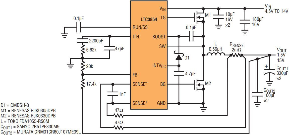
Figure 1. A 1.5V, 15A converter with a sense resistor.
Figure 2. Same converter shown in Figure 1, except with DCR sensing. The filter at R1 and C1 infers the current sense information from the inductor’s DCR.
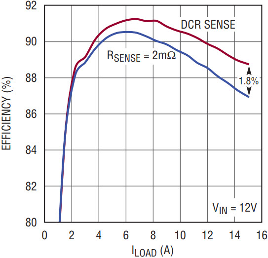
Figure 3. Efficiency of the converter with a sense resistor versus efficiency with DCR sensing. By eliminating the sense resistor, the full load efficiency goes up by almost 2%.
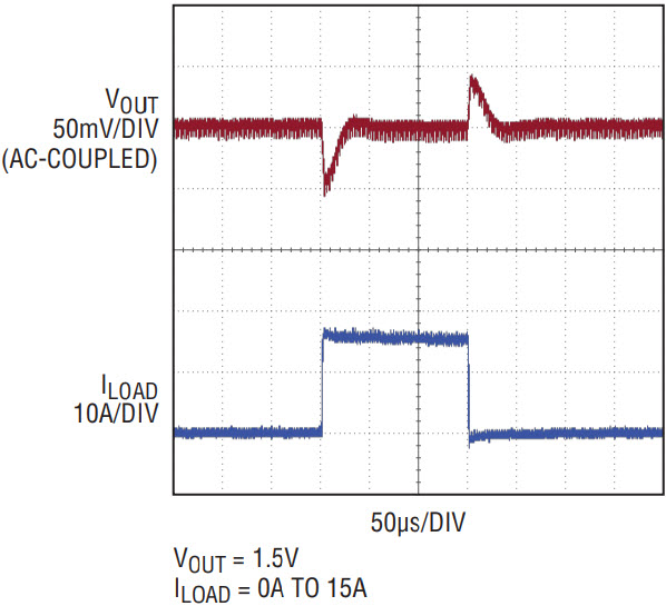
Figure 4. 50% to 100% load step 10A/DIV response of converter shown in Figure 2.
Wide Input Voltage Range Applications
The input voltage range of the LTC3854 allows it to be used in a wide variety of applications, including automotive, industrial and communications. One example of a wide input converter is the 5V, 10A converter in Figure 5, which can be used for an input voltage range of 6V to 38V. The strong gate drivers and low QG FETs allows for 94% efficiency at a 32V input voltage and 100% load as shown in Figure 6.
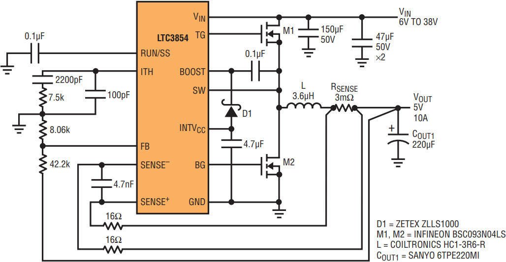
Figure 5. 5V, 10A converter with a 6V to 38V input voltage range.
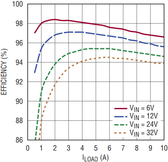
Figure 6. Efficiency of the 5V, 10A converter.
The small size and low pin count of the LTC3854 allows the control section of the 2.5V/5A converter with a 4.5V to 26V input voltage range shown in Figure 7 to fit within a 180mm2 area. Dual channel FETs are used to minimize the size of the power stage. The 400kHz switching frequency allows the use of a small 2.2µH inductor with a 7mm × 7mm footprint. The entire converter (minus the bulk input capacitor) can fit in a 430mm2 area.
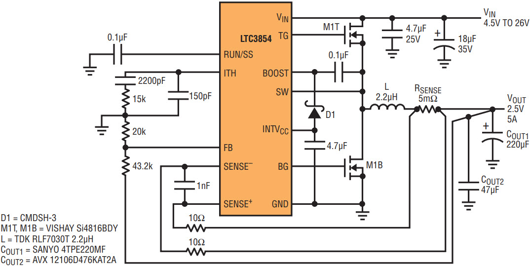
Figure 7. 2.5V, 5A converter with a 4.5V to 26V input voltage range.
Soft-Start, Low Dropout and High Step-Down Ratios
The LTC3854 features a programmable soft-start set with a capacitor on the RUN/SS pin. As the output voltage ramps up, the converter operates in discontinuous mode to prevent reverse current from flowing into the inductor. This allows the part to safely turn on into a prebiased output. After ramp-up, the part operates in continuous conduction mode. Other features are a maximum duty cycle of 97% for low dropout voltage applications, a low minimum on-time of 75ns for applications with high step-down ratios, foldback current limit in addition to the cycle-by-cycle current limit and a built-in 5V linear regulator for bias.
Conclusion
The LTC3854 delivers reliability and efficiency for cost-sensitive and space-constrained applications. The device can produce output voltages ranging from 0.8V to 5.5V over an input voltage range of 4.5V to 38V. The LTC3854’s 2mm × 3mm DFN and MSE packages, along with a 400kHz switching frequency, minimize solution size.


