SOT-23 Digitally Controlled Amplifier Puts Programmable Gain Anywhere
SOT-23 Digitally Controlled Amplifier Puts Programmable Gain Anywhere
著者
Max Hauser
2002年12月01日
Introduction
LTC6910-1 is programmable for eight gain magnitudes of 0, 1, 2, 5, 10, 20, 50, or 100 Volts/Volt—much like a classic oscilloscope amplifier plug-in or lab amplifier with a gain knob, but much smaller. This tiny DC-coupled, low-noise, self-contained amplifier, useful to low Megahertz frequencies, replaces expensive combinations of op amps and resistor arrays. The 8-lead TSOT-23 package needs no other analog components. The LTC6910-1 operates from single or dual supplies, 2.7V to 10.5V total, and generates its own ground reference for use with single supplies. A simple 3-bit CMOS digital input controls the gain.
The LTC6910-1 is an inverting voltage amplifier with a rail-to-rail output. At gains of unity and zero (digital inputs 001 and 000) it handles rail-to-rail input signals. At gains above unity (digital input 010 through 111), the input-referred noise decreases with increasing gain, as desired in a variable-gain amplifier for a wide range of input levels. When set for a gain of zero (digital input 000), the output remains active (tracking the analog-ground or AGND pin), but feedthrough from the signal input pin is low, typically –122dB at 20kHz and –100dB at 200kHz. Output noise in this zero-gain setting is typically 5.8µVRMS in a 200kHz bandwidth, which is 116dB (19 equivalent bits) below the maximum signal output at a 10V power supply. The output will source or sink 10mA into a load, and is current-limited at approximately 30mA. Typical standing supply current is 2mA at 2.7V and 3mA at 10V total VSUPPLY.
Easy to Use
The LTC6910-1 amplifier has only three analog signal pins: input, output, and an analog-ground reference (AGND), which can provide a half-supply reference for single-supply applications (Figure 1). The other pins are the power supply and the three digital input pins. These high-impedance CMOS digital inputs accept both rail-to-rail logic levels at any supply voltage, and 0V and 5V levels when the supply voltage is ±5V. Table 1 relates the 3-bit input code to the resulting voltage gain and other characteristics. (Other versions of the product are the LTC6910-2 with 0–64 binary gain code and the LTC6910-3 with 0–7 gain code.) Figure 2 shows the typical frequency response.
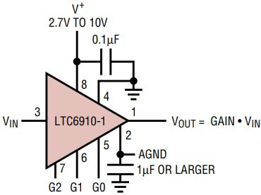
Figure 1. Single-supply programmable amplifier using LTC6910-1.
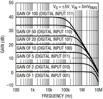
Figure 2. LTC6910-1 frequency response at non-zero gain settings.
| G2 |
G1 |
G0 |
Nominal Voltage Gain |
Maximum Input Signal (For Unclipped Output Signal) (VP-P) |
Nominal Input Impedance (kΩ) | |||
| Volts/Volt | (dB) | Dual 5V Supply | Single 5V Supply | Single 3V Supply | ||||
| 0 | 0 | 0 | 0 | –120 | 10 | 5 | 3 | (Open) |
| 0 | 0 | 1 | –1 | 0 | 10 | 5 | 3 | 10 |
| 0 | 1 | 0 | –2 | 6 | 5 | 2.5 | 1.5 | 5 |
| 0 | 1 | 1 | –5 | 14 | 2 | 1 | 0.6 | 2 |
| 1 | 0 | 0 | –10 | 20 | 1 | 0.5 | 0.3 | 1 |
| 1 | 0 | 1 | –20 | 26 | 0.5 | 0.25 | 0.15 | 1 |
| 1 | 1 | 0 | –50 | 34 | 0.2 | 0.1 | 0.06 | 1 |
| 1 | 1 | 1 | –100 | 40 | 0.1 | 0.05 | 0.03 | 1 |
Circuit Description
Internally the LTC6910-1 includes an operational amplifier, switched resistors, and CMOS decoding logic to drive the switches (Figure 3). The gain code is always monotonic: an increase in the 3-bit binary number (G2 G1 G0) increases the gain between the IN and OUT pins. For single-supply applications, an internal matched pair of 10kΩ resistors at the AGND pin generates a convenient half-supply reference voltage for input and output. The user can override this built-in analog ground reference by tying the AGND pin to a system reference voltage (within the AGND voltage range specified in the data sheet). The AGND pin presents a nominal impedance of 5kΩ due to the internal resistor pair. Digital inputs (G2 G1 G0) control the input and feedback resistances in the closed-loop amplifier.
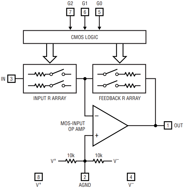
Figure 3. Block diagram of LTC6910-1.
In the design of the LTC6910-1, the lowest noise with gain variation would be achieved by varying the input R array in Figure 3. That, however, would impose a 100:1 input-resistance range for the closed-loop amplifier with a 100:1 gain range. To avoid such a wide variation of input resistance, logic in the LTC6910-1 trades off changing the input resistance and the feedback resistance (Table 2). This gain-control approach still produces near-minimal noise. When the gain setting is zero (digital input 000), switches disconnect the IN pin internally and short the feedback path in Figure 3 to reduce signal feedthrough and noise.
| Gain | RIN | RFB |
| 0 | ∞ | 0 |
| 1 | 10k | 10k |
| 2 | 5k | 10k |
| 5 | 2k | 10k |
| 10 | 1k | 10k |
| 20 | 1k | 20k |
| 50 | 1k | 50k |
| 100 | 1k | 100k |
Bandwidth of the LTC6910-1 depends on gain setting. The lower gain settings of 1, 2, and 5V/V (digital inputs 001–011) exhibit –3dB corner frequencies respectively of 7, 5, and 2.5MHz at ±5V supply (Figure 2). The gain-control strategy described above causes the gain settings from 10 to 100 (digital inputs 100–111) to show a different high-frequency response, with a constant gain-bandwidth product of approximately 11MHz.
Figure 4 is a SINAD curve showing signal output more than 100dB above combined noise and distortion, with large-signal outputs and a ±5V supply.
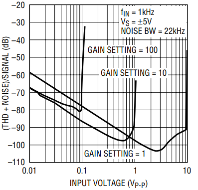
Figure 4. LTC6910-1 THD plus noise, referred to the signal output.
Applications
Expanding an ADC’s Dynamic Range
Figure 5 shows a compact data-acquisition system for wide-ranging input levels, which combines an LTC6910-1 programmable amplifier in an 8-lead TSOT-23 with an LTC1864 analog-to-digital converter (ADC) in an 8-lead MSOP. The LTC1864 ADC has 16-bit resolution and a maximum sampling rate of 250ksps. The LTC6910-1 expands the ADC’s input amplitude range by 40dB while operating from the same single 5V supply. The 499Ω resistor and 270pF capacitor couple cleanly between the LTC6910-1’s output and the switched-capacitor input of the LTC1864.
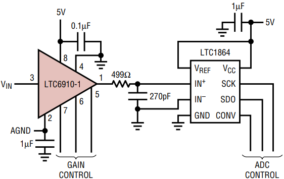
Figure 5. Expanding an ADC’s dynamic range.
The two ICs shown in Figure 5 have similar distortion performance, with total harmonic distortion (THD) levels about –90dB at 10kHz and –77dB at 100kHz. At a gain setting of 10 in the LTC6910-1 (digital input 100) and a 250ksps sampling rate in the LTC1864, a 100kHz input signal at 60% of full scale shows a THD of –75dB from the combination. 10kHz input signals under the same conditions produce measured THD values around –87dB. Noise effects (both random and quantization) in the ADC are divided by the gain of the amplifier and combined with the amplifier’s noise when referred to VIN in Figure 5. Because of this, the circuit can acquire a signal that is 40dB down from full scale of 5VP–P with an SNR of over 70dB. Such performance from an ADC alone (110dB of useful dynamic range at 250ksps) would be prohibitively expensive today.
Low Noise AC Amplifier with Programmable Gain and Bandwidth
Analog data acquisition can exploit band-limiting as well as gain, to suppress unwanted signals or noise. Tailoring an analog front end to both the level and bandwidth of each source maximizes SNR.
Figure 6 shows a block diagram and Figure 7 the practical circuit for a low-noise amplifier with gain and bandwidth independently programmable over 100:1 ranges. One LTC6910-1 controls the gain and another controls the bandwidth. An LT1884 dual op amp forms an integrating lowpass loop with capacitor C2 to set the programmable upper corner frequency. The LT1884 also supports rail-to-rail output swings over the total supply-voltage range of 2.7V to 10.5V. AC coupling through capacitor C1 establishes a fixed low frequency corner of 1Hz, which can be adjusted by changing C1. Alternatively, shorting C1 makes the amplifier DC-coupled. (When DC is not needed, however, the AC coupling suppresses low frequency noise and all amplifier offset voltages other than the low internally-trimmed LT1884 offset in the integrating amplifier, which is the second amplifier in Figure 6. If desired, another coupling capacitor in series with the input can relax the requirements on input DC level as well.)
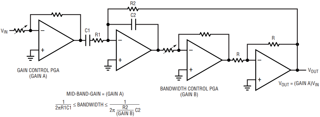
Figure 6. Low-noise AC amplifier with gain and bandwidth control.
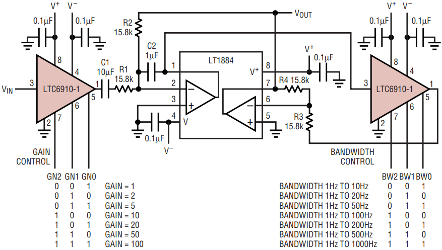
Figure 7. Practical low-noise AC amplifier with gain and bandwidth control.
Measured frequency responses (Figure 8) demonstrate bandwidth settings of 10Hz, 100Hz, and 1kHz (digital BW inputs of 001, 100, and 111, respectively) and unity gain in each case. By scaling C2, this circuit can serve other frequency ranges, such as a maximum of 10kHz with 0.1µF using LT1884 (gain-bandwidth product around 1MHz). Output signal-to-noise ratio measured with 10mVP–P input, gain of 100, and 100Hz bandwidth is 76dB; for 100mVP–P input, gain of 10, and 1000Hz bandwidth it is 64dB.
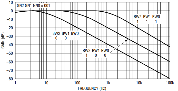
Figure 8. Measured frequency responses for Figure 7.
Conclusion
With a printed circuit footprint of only about 11mm2, the easy-to-use LTC6910-1 provides two decades of programmable DC or AC voltage gain. It can preamplify, drive loads, and introduce gain flexibility into spaces so small that, as one engineer put it, “your boss doesn’t even need to know it’s there.”


