The LT1576: 200kHz, 1.5A Monolithic Buck Converter
Introduction
The LT1576 is an improved version of the LT1376 1.5A buck switching regulator from Linear Technology. With its 200kHz switching frequency and integral switch, only a few external, surface mount components are required to produce a complete switching regulator. All the features of the LT1376 have been retained, including current mode control, external synchronization and a low current (typically 20µA) shutdown mode. Improvements have been made to reduce the start-up input supply headroom and the switching noise. The quiescent current has been reduced by one half. The feedback voltage has been lowered from 2.42V to 1.21V for low output voltage applications. Improved power-device layout also lowers the equivalent resistance of the on-chip switch from 0.3Ω to 0.2Ω.
LT1576 Features
- Constant 200kHz switching frequency
- 0.2Ω high speed switch
- 20µA shutdown current
- Uses all surface mount components
- Cycle-by-cycle current limiting
- Easily synchronizable
- Available in the SO-8 package
Circuit Description
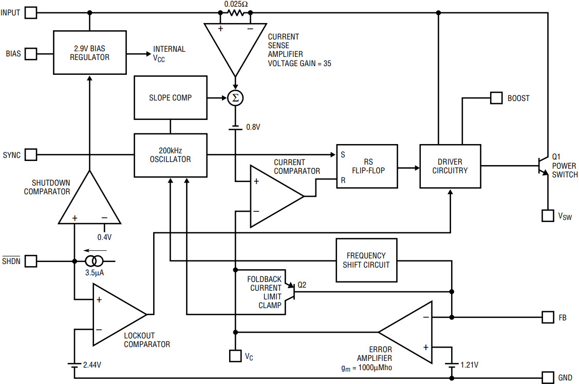
The LT1576 is a constant frequency, current mode buck converter. As shown in Figure 1, an internal clock and two feedback loops control the duty cycle of the power switch. In addition to the normal output error amplifier, a current sense amplifier monitors switch current on a cycle-by-cycle basis.

Figure 1. LT1576 block diagram.
A switch cycle starts with an oscillator pulse that sets the RS flip-flop to turn the switch on. When the switch current reaches a level set by the output of the error amplifier (that is, the VC pin), the flip-flop is reset and the switch turns off. The power stage is, in effect, turned into a programmable current source. The output current, in turn, is controlled by the error amplifier in response to changes in the output voltage.
This current mode technique means that the error amplifier controls the current delivered to the output rather than the voltage. Current mode control gives pulse-by-pulse current limiting and eases frequency compensation. A voltage mode control system will have low phase shift up to the resonant frequency of the inductor and output capacitor, then an abrupt 180° shift will occur. A current mode control system will have 90° phase shift at a much lower frequency, but will not have the additional 90° shift until well beyond the LC resonant frequency. This makes it much easier to frequency compensate the feedback loop and also gives much quicker transient response. Nonlinear slope compensation has been added to the current sense signal to prevent the subharmonic oscillation associated with current mode control when the regulator duty cycle is greater than 50%.
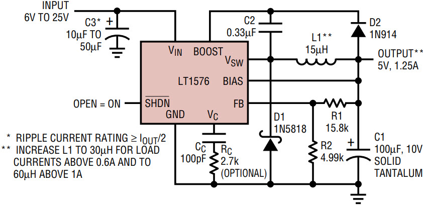
In addition to providing the output voltage feedback path to the internal error amplifier, the feedback pin, FB, provides several overload-protection functions. As the feedback pin voltage drops below 0.7V a voltage clamp is gradually applied to the VC pin, which reduces the switch current limit. Additionally, the oscillator frequency is gradually reduced to about 40kHz, which is one-fifth of the nominal 200kHz switching frequency. Because the minimum on-time for the switch remains the same, the minimum duty cycle is effectively reduced by a factor of five. This lowers the power dissipation for a shorted output condition in both the LT1576 and the catch diode, D1, shown in Figure 2. During power-up, the frequency foldback and current-limiting features of the FB pin provide a soft-start function.

Figure 2. 5V/1.25A buck converter.
High switch efficiency is attained by using the Boost pin to provide a voltage to the switch driver that is higher than the input voltage, allowing the switch to saturate. This boosted voltage is generated with an external capacitor, C2, and a diode, D2, as shown in Figure 2. The minimum boost voltage required to fully saturate the switch at maximum current has been reduced from 3.5V (LT1376) to 3V. Current used by the boost circuit is considered an efficiency loss. Supplying current from a lower voltage via the boost diode, D2, improves the efficiency. For most applications with outputs above 3V, the configuration shown in Figure 2 is optimal. Converters with lower output voltages should use the input or an alternate supply to power the boost diode.
Compared to the LT1376, the LT1576 has been improved by reducing the minimum start-up voltage at low output currents. At low output currents, there is not enough energy in the inductor at switch-off to drive the switch-node capacitance to ground. In this case, the minimum start-up voltage is the unboosted voltage drop across the output switch. Improvements made to the drive circuitry of the LT1576 have reduced this drop from 2.5V on the LT1376 to 1.5V.
The switch transition time for the LT1576 is increased to 60ns from the LT1376’s 16ns to reduce EMI and RFI without sacrificing efficiency. First, its switching frequency has been lowered to 200kHz (that of the LT1376 is 500kHz); second, efficiency is boosted by reducing the quiescent current to 1.35mA from the LT1376’s 2.5mA, and by reducing the switch on-resistance from 0.3Ω to 0.2Ω.
Most of the circuitry of the LT1576 operates from an internal 2.9V bias supply. The bias regulator normally draws power from the regulator input pin, but if the bias pin is connected to an external voltage higher than 3V, bias power is drawn from the external source (typically the regulated output voltage). This improves efficiency if the bias pin voltage is lower than regulator input voltage.
On some versions of the LT1576, an external clock signal (up to 400kHz) can be fed into the SYNC pin to increase the internal oscillator frequency or synchronize it to a system clock. The synchronization feature is defeated when the FB pin voltage is below 0.7V. This allows the frequency foldback function to work during start-up.
Two comparators are connected to the shutdown pin. The first comparator, with a threshold of 2.44V, disables the output switch and can be used as an undervoltage lockout level. The second comparator, with a threshold of 0.4V, puts the device into a low quiescent current shutdown state, where quiescent current drops to just 20µA.
Typical Application: 5V/1.25A Buck Converter
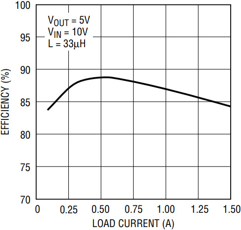
Figure 2 shows a typical buck converter using the LT1576 with a 6V to 25V input range, a 5V output and 1.25A output current capability. Due to the low on-resistance of the on-chip switch, the converter efficiency remains high over a wide range of output currents, as shown in Figure 3. To achieve high efficiency, both the BIAS pin and the boost circuit are powered from the 5V output.

Figure 3. Efficiency of Figure 2’s circuit.
The choice of the surface mount inductor, L1, is affected by several factors, including the maximum current, core and copper losses, size and cost. A high value, high current inductor gives the highest output current with the lowest ripple, at the expense of a large physical size and cost. Lower inductance values tend to be physically smaller and have higher current ratings. They are less expensive, but the output ripple current, and hence the output ripple voltage, increases.
The input capacitor C3 must be rated to absorb all switching current ripple. The ripple current can be as high as IOUT/2, so low ESR tantalum capacitors are needed. The ripple current rating on the input capacitor must be observed to ensure reliable operation. The ripple current at the output capacitor is lower, but its ESR still needs to be low to limit the output ripple voltage.
The voltage drop across the catch diode D1 has a significant effect on overall converter efficiency, especially at higher input voltages when the switching duty cycle is low. For good electrical performance, D1 must be placed close to the LT1576.
Loop Compensation
For most LT1576 applications, the suggested frequency compensation is a 100pF capacitor (CC) from the VC pin to ground. The following description of the loop frequency response characteristics is provided as an aid in optimizing loop compensation.
In an LT1576 closed-loop regulator system, two low frequency poles are formed by the output capacitor and the compensation capacitor. A high frequency zero is formed by the output capacitor and its ESR. The location of this zero varies with the type of output capacitor. To stabilize the regulator, this zero must bring the loop phase up before the phase contributed by the two low frequency poles reaches −180° at unity gain. If loop stability must be improved, another high frequency zero can be formed by adding a resistor, RC, (typically around 3k) in series with compensation capacitor CC (see Figure 2). The unity-gain phase margin can be adjusted by changing the value of RC (and hence, the location of the zero). Although it solves the loop-stability problem, this added resistor occasionally causes a large-signal subharmonic problem in the control loop. The output ripple voltage feeds back through the error amplifier to the VC pin, changing the current trip point of the next cycle. Changing the value of RC also changes the high frequency gain of the error amplifier. If the loop frequency response gain at the switching frequency is high enough, the output ripple voltage can appear at the VC pin with enough amplitude to interfere with the proper operation of the regulator. This subharmonic problem can be solved by adding a second capacitor—typically from 1nF to 3nF—directly from the VC pin to ground to form a pole at one-fifth the switching frequency. This capacitor provides significant attenuation of the switching ripple but does not add unacceptable phase shift at the loop’s unity-gain frequency.
PCB Layout
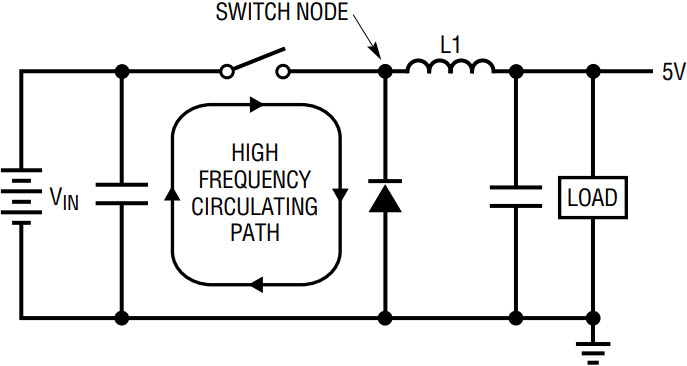
All high current, high speed circuits require careful layout to obtain optimum performance. When laying out the PCB, keep the trace length around the high frequency switching components, shown in Figure 4, as short as possible. This minimizes the EMI and RFI radiation from the loop created by this path. These traces have a parasitic inductance of approximately 20nH/inch, which can cause an additional problem at higher operating voltages. At switch-off, the current flowing in the trace inductance causes a voltage spike. This is in addition to the input voltage across the switch transistor. At higher currents, the additional voltage can potentially cause the output switching transistor to withstand more than its absolute maximum voltage rating.

Figure 4. High speed switching path.
Conclusion
The LT1576 makes a very compact, low parts count, 1.5A DC/DC converter without the need for separate control and power devices. Compared to the existing LT1376, this new part has been improved to reduce the startup input supply headroom and switching noise. The quiescent current has been reduced from 2.5mA to 1.35mA. Improved power-device layout also lowers the on-chip switch on-resistance from 0.3Ω to 0.2Ω. Because of the former two factors, efficiency is greatly improved. Additionally, the feedback voltage has been lowered from 2.42V to 1.21V, which will meet the requirements for lower output voltage applications.


