LT1533 Ultralow Noise Switching Regulator for High Voltage or High Current Applications
LT1533 Ultralow Noise Switching Regulator for High Voltage or High Current Applications
著者
Jim Williams
1998年02月01日
The LT1533 switching regulator1, 2 achieves 100µV output noise by using closed-loop control around its output switches to tightly control switching transition time. Slowing down switch transitions eliminates high frequency harmonics, greatly reducing conducted and radiated noise.
The part’s 30V, 1A output transistors limit available power. It is possible to exceed these limits while maintaining low noise performance by using suitably designed output stages.
High Voltage Input Regulator
The LT1533’s IC process limits collector breakdown to 30V. A complicating factor is that the transformer causes the collectors to swing to twice the supply voltage. Thus, 15V represents the maximum allowable input supply. Many applications require higher voltage inputs; the circuit in Figure 1 uses a cascoded3 output stage to achieve such high voltage capability. This 24V to 5V (VIN = 20V– 50V) converter is reminiscent of previous LT1533 circuits, except for the presence of Q1 and Q2.4 These devices, interposed between the IC and the transformer, constitute a cascoded high voltage stage. They provide voltage gain while isolating the IC from their large drain voltage swings.

Figure 1. A low noise 24V to 5V converter (VIN = 20V–50V): cascoded MOSFETs withstand 100V transformer swings, permitting the LT1533 to control 5V/2A output.
Normally, high voltage cascodes are designed to simply supply voltage isolation. Cascoding the LT1533 presents special considerations because the transformer’s instantaneous voltage and current information must be accurately transmitted, albeit at lower amplitude, to the LT1533. If this is not done, the regulator’s slew-control loops will not function, causing a dramatic output noise increase. The AC-compensated resistor dividers associated with the Q1–Q2 gate-drain biasing serve this purpose, preventing transformer swings coupled via gate-channel capacitance from corrupting the cascode’s waveform transfer fidelity. Q3 and associated components provide a stable DC termination for the dividers while protecting the LT1533 from the high voltage input.
Figure 2 shows that the resultant cascode response is faithful, even with 100V swings. Trace A is Q1’s source; traces B and C are its gate and drain, respectively. Under these conditions, at 2A output, noise is inside 400µV peak.

Figure 2. MOSFET-based cascode permits the regulator to control 100V transformer swings while maintaining a low noise 5V output. Trace A is Q1’s source, Trace B is Q1’s gate and Trace C is the drain. Waveform fidelity through cascode permits proper slew-control operation.
Current Boosting
Figure 3 boosts the regulator’s 1A output capability to over 5A. It does this with simple emitter followers (Q1– Q2). Theoretically, the followers preserve T1’s voltage and current waveform information, permitting the LT1533’s slew-control circuitry to function. In practice, the transistors must be relatively low beta types. At 3A collector current, their beta of 20 sources ≈150mA via the Q1–Q2 base paths, adequate for proper slew-loop operation.5 The follower loss limits efficiency to about 68%. Higher input voltages minimize follower-induced loss, permitting efficiencies in the low 70% range.

Figure 3. A 10W low noise 5V to 12V converter: Q1–Q2 provide 5A output capacity while preserving the LT1533’s voltage/current slew control. Efficiency is 68%. Higher input voltages minimize follower loss, boosting efficiency above 71%.
Figure 4 shows noise performance. Ripple measures 4mV (Trace A) using a single LC section, with high frequency content just discernible. Adding the optional second LC section reduces ripple to below 100µV (trace B), and high frequency content is seen to be inside 180µV (note ×50 vertical scale-factor change).
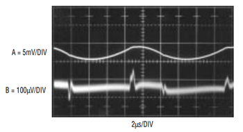
Figure 4. Waveforms for Figure 3 at 10W output: Trace A shows fundamental ripple with higher frequency residue just discernible. The optional LC section results in Trace B’s 180µVP-P wideband noise performance.
Notes
1 Witt, Jeff. The LT1533 Heralds a New Class of Low Noise Switching Regulators. Linear Technology VII:3 (August 1997).
2 Williams, Jim. LTC Application Note 70: A Monolithic Switching Regulator with 100µV Output Noise. October 1997.
3 The term “cascode,” derived from “cascade to cathode,” is applied to a configuration that places active devices in series. The benefit may be higher breakdown voltage, decreased input capacitance, bandwidth improvement or the like. Cascoding has been employed in op amps, power supplies, oscilloscopes and other areas to obtain performance enhancement.
4 This circuit derives from a design by Jeff Witt of Linear Technology Corp.
5 Operating the slew loops from follower base current was suggested by Bob Dobkin of Linear Technology Corp.
著者について
James M. Williams(1948年4月14日~2011年6月12日)はマサチューセッツ工科大学(1968年~1979年)、Philbrick、National Semiconductor(1979年~1982年)、Linear Technology Corporation(LTC)(1982年~2011年)でアナログ回路設計者ならびに技術文書の著者を務めていました。同氏は、書籍5冊、National Semiconductorの...


