Highly Integrated USB Power Manager with Li-Ion Charger and Three Step-Down Switching Regulators in 4mm × 4mm QFN
Highly Integrated USB Power Manager with Li-Ion Charger and Three Step-Down Switching Regulators in 4mm × 4mm QFN
著者
Amit Lele
2007年06月01日
Introduction
Mobile technology has radically changed the way we acquire, share and disseminate information. Modern, feature-rich handheld and portable devices require several power management circuits, including a battery charger, multiple step-down switching regulators and low power LDOs for watchdog circuitry. If each of these functions is served by a separate power supply IC, each IC (and its external components) occupies valuable board space, consumes battery-draining quiescent current and significantly increases the overall development and material costs of the device. The LTC3557 solves this problem by bringing all power management functions into a single device. It combines a full featured USB power manager, a Li-ion battery charger, three high frequency step-down switching regulators and a 3.3V always-on LDO in a single 4mm × 4mm QFN package.
Features
The LTC3557 is a highly integrated power management and battery charger IC for single cell Li-Ion/Polymer battery applications. Table 1 highlights some of the key features of the LTC3557.
| Feature | Benefits |
| PowerPath Control | Allows seamless transition between input power sources (Li-Ion battery, USB, wall adapter or high voltage buck regulator) to supply system load. |
| WALL Input | Provides power from 5V wall adapter directly to system load through an external low impedance PFET |
| USB Input | Precision input current limit which communicates with the battery charger to ensure that input current never violates the USB specification |
| High Voltage Buck Control with Bat-Track™ | Controls external HV buck to expand input voltage range up to 38V. The Bat-Track feature allows efficient charging of the battery to minimize heat dissipation in the application |
| Li-Ion Charger | Uses constant current/constant voltage architecture with thermal regulation for optimal charging. Preset float voltage accurate to 0.85%. |
| Temperature qualified charging using NTC | Disables charging of the battery under extreme temperature conditions outside a programmable range |
| Internal Safety Timer | Limits maximum charge cycle to 4 hours |
| CHRG Fault Reporting | Four modes of CHRG pin including ON, OFF, Slow Blink and Fast Blink to report various operating states |
| Three High Efficiency Step-Down Switching Regulators | High frequency switching (2.25MHz) stays out of the AM band and enables use of tiny inductors. Internally compensated to save valuable board space. User-programmable output voltages with external resistor divider. Power on Reset output for power sequencing. |
| Always on 3.3V LDO | Ultra low quiescent current 3.3V LDO for real time clock, standby power, pushbutton control, etc. |
The LTC3557 can derive power from a current limited input such as USB. The programmable current limit is set by a single external resistor (RCLPROG) on the CLRPOG pin and the logic state of ILIM0 and ILIM1 pins. Table 2 shows the different operating modes of the input current limit.
| ILIM1 | ILIM0 | IBUS(LIM) |
| 0 | 0 | 100mA(1x) |
| 0 | 1 | 1A(10x) |
| 1 | 0 | SUSPEND |
| 1 | 1 | 500mA(5x) |
The 1A (10x) mode is reserved for use with a higher current input power supply such as an AC wall adapter. Alternatively, power can be directly provided to the system load (VOUT) via an external PFET connected in series with an AC wall adapter. The input supply range can be expanded by using an appropriate high voltage buck regulator as shown in Figure 1. The LTC3557 takes over the control of buck regulator via the VC pin and sets the VOUT pin voltage at a fixed offset above the battery voltage. This Bat-Track feature charges the battery at the highest efficiency. Absent all other input power sources, the battery provides power to the system (VOUT) through an internal 200mΩ ideal diode. An optional external <50mΩ ideal diode can be used to minimize the voltage drop from BAT to VOUT in high current applications.
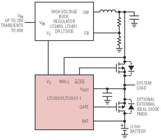
Figure 1. High voltage buck control using VC.
The LTC3557 charger circuitry uses constant current/constant voltage architecture to optimize the charging of the battery. The battery charge current is set by an external resistor (RPROG) connected to the PROG pin as follows:

The LTC3557 includes several safety mechanisms to handle situations when the available input current is less than the programmed charge current. This allows the system designer to set the charge current based on normal operating conditions rather than reducing the charging current to account for worst-case scenarios. These safety mechanisms are explained in more detail in the “Getting the Priorities Right” section below.
The LTC3557 includes three step-down switching regulators capable of delivering up to 600mA. Additionally, an always-on LDO with fixed 3.3V output voltage can deliver up to 25mA of load current. This can be used to power watchdog circuitry or other low power circuitry.
A Typical Application
Figure 2 shows a typical application using the LTC3557. In this configuration, the LTC3557 automatically switches between the high voltage buck power supply or the USB/5V wall adapter. The USB input current is programmed to nominal value of 476mA using a 2.1k resistor on the CLPROG pin. The charge current is programmed to 500mA using a 2k resistor on PROG pin. The resistor network on the NTC pin sets the battery charging temperature range from 0°C to 40°C based on R-T curve 1 characteristics for the 100k NTC thermistor. An LED on the CHRG pin provides battery charging and status information.
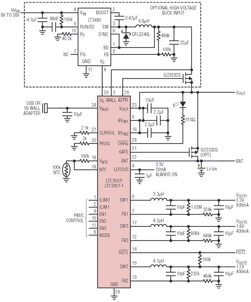
Figure 2. Typical application circuit for LTC3557.
VOUT1 is set to 3.3V to drive higher power applications such as I/O or disk drives. VOUT3 is set to 1.8V to drive medium power applications while VOUT2 is set to 1.2V to drive a microprocessor core. The RST2 output can be used to provide power supply sequencing using the PMIC control pins. The optional external ideal diode can be used to provide a lower impedance path from BAT to VOUT for applications that draw heavy loads from the battery.
Safety Timer and Automatic Recharge
An internal safety timer shuts off all charge current to the battery after 4 hours of charging. As long as the load current at VOUT does not exceed the current available from the external power source, the battery remains fully charged. If the load current at VOUT exceeds the current available from the external power source, the extra current is pulled from the battery. This causes the battery to discharge and if the battery voltage drops below 100mV of its float voltage (4.2V for LTC3557 or 4.1V for LTC3557-1), an automatic recharge cycle is initiated.
Getting the Priorities Right
The USB specification has very strict restrictions on the maximum current that can be pulled out of the bus. For this reason the LTC3557 provides load prioritization on the system load (VOUT) as shown in Figure 3. Power is always prioritized at VOUT and the battery charge current is automatically dialed back so that the USB current limit is never exceeded. This feature enables the battery charge current to be programmed to normal operating conditions rather than worst case load on VOUT.
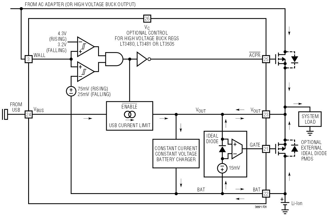
Figure 3. Simplified PowerPath block diagram.
The charge current is also automatically dialed back at high temperatures to prevent the part from overheating. Additionally, if VOUT starts to drop due to heavy load, the charge current is dialed back to maintain VOUT near VBUS. If the system load exceeds the programmed USB current limit, the additional current needed is drawn from the battery. Power provided directly to VOUT pin via the WALL input is prioritized over USB power as USB power is current limited.
Status Symbols
The CHRG pin provides valuable information regarding the status of battery charging. The CHRG pin is an open drain output that is pulled low during a normal charge cycle. When the charge current reduces to one tenth of the programmed value of charge current (C/10) the CHRG pin is let go and is pulled high by the external pull-up device to the appropriate rail voltage. Two Fault modes are also encoded on to the CHRG output. If the battery voltage fails to rise above 2.85V even after charging it for a half hour, it is deemed to be a bad battery and this fault is reported at the CHRG pin as a fast blink (6Hz signal modulated at 35kHz). Temperature qualified charging can be enabled with an external resistor divider on the VNTC and NTC pins as shown in Figure 4. This defines a range of temperatures for charging the battery and is a function of the thermal characteristics of the NTC resistor. When the battery temperature is outside the defined range, an NTC fault is indicated at the CHRG pin by a slow blinking (1.5Hz signal modulated at 35KHz).
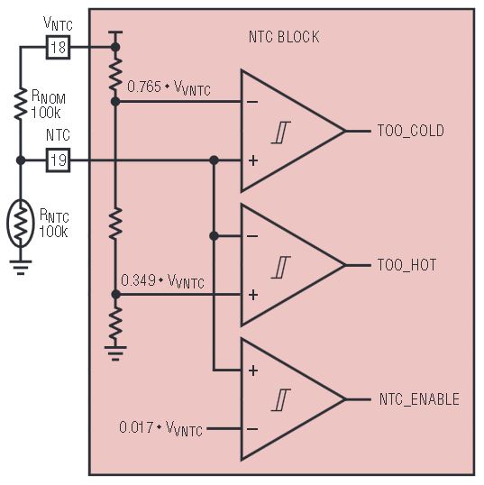
Figure 4. Temperature qualified charging using NTC.
Step-Down Switching Regulators
The LTC3557 includes three internally compensated 2.25MHz constant-frequency current-mode step-down switching regulators providing 600mA, 400mA and 400mA each. All step-down switching regulators can be programmed for a minimum output voltage of 0.8V and can be used to power a microcontroller core, microcontroller I/O, memory or other logic circuitry. Figure 5 shows the step-down switching regulator application circuit. The full-scale output voltage for each step-down switching regulator is programmed using a resistor divider as shown in the figure such that

Typical values of R1 are in the range of 40kΩ to 1MΩ. The capacitor CFB cancels the pole created by the feedback resistors and the input capacitance of the FB pin, and also helps to improve transient response for output voltages much greater than 0.8V. A value of 10pF is recommended for CFB for most applications.
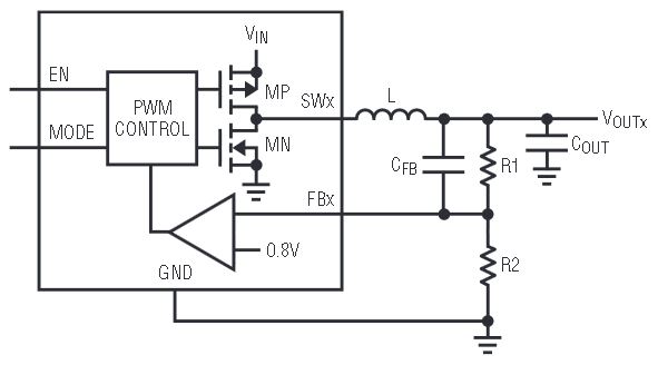
Figure 5. Buck converter application circuit.
All three of the step-down switching regulators support 100% duty cycle operation (low dropout mode) when the input voltage drops very close to the output voltage. Each regulator can be individually enabled through its respective enable pin.
A single MODE pin sets the three voltage regulators in a high efficiency Burst Mode operation (MODE = 1) or low ripple pulse-skip mode (MODE = 0). For high enough load currents, in either mode, the step-down switching regulators automatically switch into constant frequency PWM mode operation. The high 2.25MHz switching frequency allows the use of tiny power inductors and stays out of the AM Band.
The step-down switching regulators also include soft-start to limit inrush current when powering on, short-circuit current protection and switch node slew rate limiting circuitry to reduce EMI radiation. It is recommended that the step-down switching regulator input supplies (VIN1 and VIN2) be connected to the system supply pin (VOUT). This allows the undervoltage lockout circuit on the VOUT pin to disable the step-down switching regulators from operating outside the specified voltage range.
Power Sequencing using RST2
The RST2 open drain output responds to step-down switching regulator 2 and issues a Power ON reset signal 230ms after the feedback voltage (FB2) rises to within 8% of its final value. This output can be pulled to a desired voltage level using an external pull-up resistor and used for sequencing power rails. For example, it could be used to drive the enable inputs of the other switching regulators.
Conclusion
In summary, the LTC3557 provides a highly integrated solution for handheld and mobile applications in a compact 4mm × 4mm QFN package. The variety of input power sources and externally programmable output voltages make it ideally suited for a broad range of applications. The feature rich Li-Ion charger provides protection against several real-world fault conditions while the versatile high frequency step-down switching regulators provide high efficiency power.


