Efficient, Flexible Boost Converter Fits into Charge-Pump Footprint
Introduction
Handheld devices often use low power step-up DC/DC converters to power displays, LEDs and I/O circuitry, or to charge alternate power sources. Capacitive charge-pumps or inductor-based boost converters are the two most common solutions to step-up conversion, and each has certain advantages and trade-offs. A charge-pump converter offers a simple, compact solution, but it has a limited range of VIN to VOUT ratios, such as 3.3V to 5V. A traditional boost converter offers more efficient operation and a greater range of step-up ratios, but boost solutions typically take more space, and systems issues such as inrush current and short circuit protection are often solved with added external circuitry.
The LTC3459 is a small, synchronous boost converter that addresses many issues found in a traditional boost converter. The LTC3459 offers Burst Mode operation for high efficiency at light loads and a simple design (no compensation network). The internal MOSFET switches save space, protect circuitry by controlling inrush current during start-up, and are robust enough to survive a continuous short-circuit at the output. When the LTC3459 is shutdown the output is disconnected from the input, removing voltage from the load and reducing the drain on the battery.
Tiny Solution Size
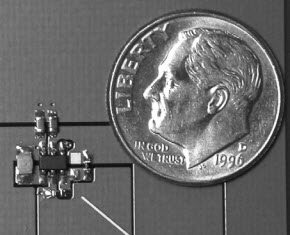
A demonstration board with a complete LTC3459 ThinSOT solution is shown in Figure 1. The input and output capacitors, used to minimize voltage ripple on the supply rails, are 0603 X5R ceramics. Since the converter operates with a low peak current of approximately 75mA, a 0805 miniature inductor from Murata is chosen to maintain a footprint similar to a charge-pump. External feedback resistors and pads for an optional feed-forward capacitor complete the design. The resulting solution size is approximately 30mm2.

Figure 1. Typical solution size with LTC3459 ThinSOT™ boost converter.
Efficiency and Operating Range
The LTC3459 has an input voltage range from 1.5V to 5.5V and an output that is programmable up to 10V. VOUT can be regulated below VIN with this IC, an important consideration for battery-powered devices. The converter is designed to maintain good efficiency over the Li-Ion battery range (2.7V to 4.2V) or a 2-cell alkaline input (2.0V to 3.3V).
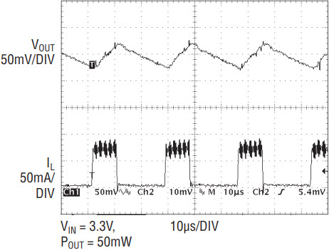
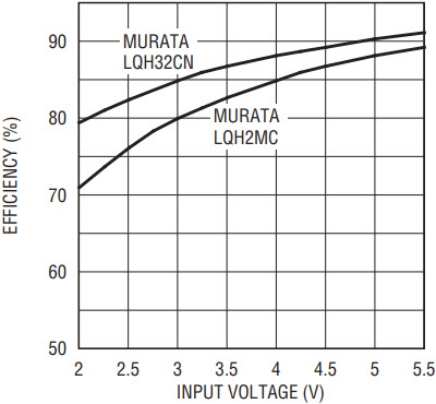
Figure 2 shows an application where the LTC3459 is used to provide a 7V, 50mW bias for an organic LED display (OLED). VOUT ripple (AC coupled) and inductor current waveforms are shown in Figure 3, where Figure 4 shows efficiencies of this application with a 2V–5.5V input. Efficiency was taken with two 22µH Murata inductors: one from the LQH2MC series (shown in Figure 1) and a slightly larger inductor from the LQH32CN series. The larger inductor gives about 5% better efficiency, due to lower DC resistance and losses in the core. Since the LTC3459 uses Burst Mode operation with only 10µA of quiescent current, the efficiencies shown in Figure 4 are relatively constant with load current down to 100µA. If the minimum input voltage is increased to 3V, a 100mW load can be supported in this application.

Figure 2. Powering a 7V, 50mW OLED from a 2V–5.5V input.

Figure 3. VOUT ripple and inductor current for the OLED application.

Figure 4. OLED efficiency comparison for two inductor types with a 7V, 50mW load.
Charging a SuperCap
The output disconnect function in the LTC3459 allows peak current to be controlled during startup or when VOUT is less than VIN. This makes the LTC3459 an ideal candidate for charging a backup source such as a SuperCap®. Figure 5 shows an application where the LTC3459 is used to charge a 2F, 5V ultracap from a 3.3V or battery input. Once the SuperCap is charged to 5V, it can be used to backup the 3.3V supply rail (through an LTC1844-3.3 VLDO in this example) if the primary power source is removed.

Figure 5. SuperCap-based backup supply using the LTC3459 and LTC1844.
The LTC3459’s operation in this application depends on the levels of VIN and VOUT. When VOUT is less than approximately 3.5V, the body of the internal synchronous P-channel MOSFET rectifier is connected to VIN (forming a PNP transistor) and the SW pin rises a Vbe above VIN when current is delivered to the load. While efficiency is lower in this mode of operation, current to the SuperCap is controlled, preventing any damaging effects of inrush current. When VOUT is greater than 3.5V, normal boost mode operation and efficiency begin, with the P-channel MOSFET acting as a synchronous switch. Average input current is approximately 50mA during charging, while the current delivered to the SuperCap varies somewhat with duty cycle. Once the SuperCap is charged to 5V, the LTC3459 begins to regulate and the input current is reduced to the amount required to support the load and/or self discharge of the SuperCap.
Conclusion
The LTC3459 simplifies and shrinks the traditional boost converter without compromising flexibility and efficiency. The device itself takes care of typically challenging boost converter design issues such as output disconnect, inrush current limiting, and short circuit protection. The LTC3459’s wide input voltage range makes it compatible with many different battery sources, and its output voltage can be programmed to satisfy the requirements of a wide variety of applications.
SuperCap is a registered trademark of Baknor Industries


