Easy Multivoltage Layout with Complete Dual and Triple Output Point-of-Load μModule Regulators in 15mm × 15mm Packages
Easy Multivoltage Layout with Complete Dual and Triple Output Point-of-Load μModule Regulators in 15mm × 15mm Packages
2009年09月01日
Introduction
Imagine a multivoltage printed circuit board so space-constrained that even the most experienced layout engineer would shiver at the thought of putting together the puzzle of components for DC/DC conversion. A typical multivoltage solution either incorporates a single multioutput DC/DC regulator IC or several independent regulators. Either solution requires a number of discrete support components, such as inductors, capacitors and resistors. Since there is a wide range of available small, high performance ICs, this type of system design is typical. Unfortunately, even the best of these regulators require careful placement of support components to take into account both electrical effects and heat dissipation concerns.
Board-mounted point-of-load (POL) DC/DC power supplies are becoming increasingly popular as they simplify board assembly and reduce external components. The ideal setup would have nearly everything packaged into a single chip, with the following features in a board-mounted POL power supply.
- Minimal components—far fewer than a discrete solution
- Multiple voltage input and output rails with available current sharing
- Independent input and output regulation for application flexibility
- Worry-free thermal dissipation
- Low noise output
- High efficiency
Complete Dual and Triple DC/DC Regulators in IC Form Factors
The LTM4614 and LTM4615 cure the headaches inherent in laying out multivoltage systems for space-constrained applications. Both devices are point-of-load power supplies in a 15mm × 15mm × 2.8mm LGA surface mount packages, each with two switching 4A DC/DC regulators (see Figure 1). The LTM4615 adds a VLDO™ (very low dropout) linear regulator, making it a triple output voltage regulator. The MOSFETs, inductor and other support components are all built into the package, so layout involves little more than finding a 15mm × 15mm space on the board.

Figure 1. The LTM4614 dual output and LTM4615 triple output μModule regulators.
The two switching regulators operate from input voltages between 2.375V to 5.5V (6V peak) and each delivers a resistor-set output voltage of 0.8V to 5V at 4A of continuous current (5A peak). They operate at a 1.25MHz switching frequency using current mode architecture to enable fast transient response to line and load changes with no sacrifice in stability. The output voltages can track each other or another voltage. Other features include low output voltage ripple and excellent thermal dissipation.
The LTM4615’s VLDO regulator accepts input voltages from 1.14V to 3.5V and is capable of up to 1.5A of output current with an adjustable output range of 0.4V to 2.6V, also via a resistor. The VLDO regulator has a low voltage dropout of 200mV at maximum load. The regulator can be used independently or used in conjunction with either of the two switching regulators to create a high efficiency, low noise, large ratio step down supply—simply tie one of the switching regulator’s outputs to the input of the VLDO regulator.
Flexible Input and Output Combinations
The LTM4614 and LTM4615 power supplies can be used in a wide range of input and output combinations; from entirely independent inputs and outputs to single input, single output designs where a parallel, current sharing design enables high current applications.
Independent Inputs and Outputs
The LTM4614’s and LTM4615’s separate inputs and outputs make it possible to run each internal regulator from a different input. Figure 2 shows an application converting 5V, 3.3V, and 1.5V inputs to 1.8V, 2.5V, and 1V output voltage rails, respectively.

Figure 2. Very few components are required for a triple independent input (5V, 3.3V, 1.5V) to triple output (1.8V, 2.5V, 1V) μModule regulator design.
Single Input, Independent Outputs
For designs that only have a single source input voltage, tie the input voltage rails together as in Figure 3, where both inputs run off the 5V source input voltage, for example. If the input source voltage is too high for the VLDO regulator and a separate source is not available, the VLDO input of the LTM4615 can be tied to one of the outputs as in Figure 4.

Figure 3. Single switching regulator input (5V) and single linear regulator input (1.5V) to triple output (1.8V, 2.5V, 1V) μModule regulator design.
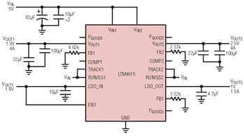
Figure 4. Single input (5V) to dual output (1.8V, 2.5V), with the linear regulator serving up a third output (1V) from an input tied to VOUT1 (1.8V).
Single Input, Current-Shared Outputs
For designs that require more than the 4A-per-regulator maximum output current, the two switching regulators can be tied together to form a paralleled, single-output 8A design (see Figure 5). This design also has efficiency advantages over a higher-current rated, single switching regulator design. In the case of the LTM4615, the VLDO linear regulator can still be used as an independent supply.

Figure 5. The two switching regulators share the load in a 1.8V/8A output system. (For an alternative 8A μModule regulator, see the LTM4608A data sheet.)
Power Sharing Multiple Inputs, Current-Shared Outputs
When a single input source cannot provide enough current to support a high power, single current-shared output, another input, even at a different voltage, can be used to provide the additional current. Figure 6 shows two different input voltages to power a single voltage current sharing output.

Figure 6. The two switching regulators combine available power from two independent input voltage rails (3.3V and 5V) and produce a single current-shared 1.8V/8A output.
High Efficiency and Low Noise Output Voltage Ripple
The LTM4615 is capable of operating with all three regulators at full load while maintaining optimum efficiency. Figure 7 shows a typical LTM4615 design for a 3.3V input to three outputs. In Figure 7, the VLDO input is driven by VOUT2. The expected efficiency of this design is shown in Figure 8. Expect similar efficiency results with the LTM4614 minus the additional VLDO output.

Figure 7. A single input, 3-output design using the LTM4615’s VLDO regulator.

Figure 8. Efficiency of the circuit in Figure 7.
To minimize the number of support discrete components, both LTM4614 and LTM4615 include internal ceramic capacitors. Layout problems associated with placing external support components are eliminated. Additional output capacitors are needed if load steps from 0A to the full 4A are expected and if the input source impedance is compromised by long inductive leads or traces.
The benefit of combining a switching regulator with a linear regulator is the noise reduction benefits that can be gained. By utilizing the switching regulator’s high efficiency step-down function and feeding its output to the input of the VLDO regulator, an exceptionally low ripple output is produced—ideal for systems that require a particularly clean signal. Figure 9 shows the low output voltage ripple for all three outputs. The VLDO regulator provides a very low noise 1V supply as it is driven by the output of the 1.2V switching regulator.

Figure 9. Low voltage ripple on all three outputs of Figure 7.
Thermally Enhanced Packaging
The LGA packaging allows heat sinking from both the top and bottom. From the bottom, the PCB copper layout draws heat away from the part and into the board. A heat sink can be placed on top of the device, such as a metal chassis, to promote good thermal conductivity. Figure 10 shows that thermal dissipation is well-balanced between the two switching regulators.

Figure 10. Top view thermal imaging of the unit at full load in an ambient temperature environment with no airflow. Cursors 1 and 3 mark the temperature hot spots on the unit for each of the two switching regulators. Both temperatures are fairly similar indicating balanced thermal conductivity.
Output Voltage Tracking
Tracking can be programmed using the TRACK1 and TRACK2 pins. To implement coincident tracking, at the slave’s TRACK pin, divide the master regulator’s output with a resistor divider that is the same as the slave regulator’s feedback divider. Figure 11 shows a tracking design and Figure 12 shows the output. VOUT2 tracks VOUT1 in master-slave design with both outputs ramping up coincidently. The smooth start-up time is attributed to the soft-start capacitor.

Figure 11. Output voltage tracking design example.

Figure 12. Start-up waveforms for the circuit in Figure 11.
Conclusion
The cumbersome designs typical of multivoltage regulation are a thing of the past. The LTM4614 and LTM4615 μModule multiple-output regulators can be easily fit into space-constrained system boards with far fewer components than discrete solutions. The dual-output LTM4614 μModule regulator and triple-output LTM4615 are small in size, have excellent thermal dissipation and have high efficiency. Independent input and output voltage rails give these μModule regulators unmatched flexibility. They can be used in a variety of input-output combinations, including input and output current sharing, output voltage tracking, and low noise output.
著者について
Eddie Beville is a power module design manager responsible for the design and development of the μModule® family. Eddie holds a BS in Electronic Engineering Technology from Chapman University, Orange, California. Eddie enj...
Alan Chern is a former associate design engineer at Linear Technology (now part of Analog Devices). He was responsible for supporting uModule® Power products in design, testing, demo board production, and product evaluatio...


