Dual/Triple Power Supply Monitor for Undervoltage and Overvoltage on Positive and Negative Supplies
Dual/Triple Power Supply Monitor for Undervoltage and Overvoltage on Positive and Negative Supplies
2006年06月01日
Introduction
An accurate power supply monitor can signal when a supply overvoltage or undervoltage condition threatens to cause system failures, allowing the system to deal with the situation gracefully.
The LTC2909 is a highly customizable monitoring solution with adjustable input thresholds, input polarity selection, a multimode reset timer, and an open-drain RST output. Adjustable input thresholds allow the user to set any trip threshold for the comparator, subject only to the accuracy limitations of the part, instead of having to pick from a factory-set limited collection of thresholds.
Each adjustable input can be configured in either polarity, allowing it to monitor negative or positive supply voltages for undervoltage or overvoltage. Polarity selection is controlled by simple connection of the SEL pin—no external components required.
The multimode timer pin can be configured a number of ways to suit a large variety of applications, allowing full control over the reset timeout, elimination of the external timing capacitor, or removal of the timeout altogether. The RST pin is an open-drain output—it can be pulled up to an appropriate voltage for the device receiving the RST signal, independent of the supply for the LTC2909. The output can be wired-OR connected with other supervisors or other open-drain logic, allowing any of a number of conditions to issue a reset.
Minimal Space Required
Figure 1 shows how the LTC2909, with just a few components, can monitor a 24V supply for both undervoltage and overvoltage. Almost any two reset conditions in any system can be monitored by appropriate connection of the LTC2909. The small size of the LTC2909 (available in 8-pin 3mm × 2mm DFN and TSOT-23 packages) keeps the monitoring solution small, and the high accuracy of the part keeps system uptime high without sacrificing reliability. The separate VCC pin of the LTC2909 incorporates a shunt regulator, which allows the part to be powered from any high availability supply, even a high voltage rail. Furthermore, the low quiescent current consumed by the LTC2909 makes it suitable for low power applications like battery powered handheld devices.
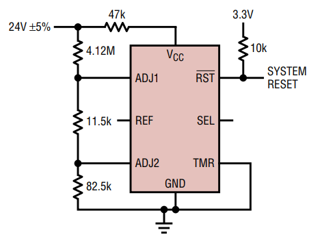
Figure 1. A 24V undervoltage and overvoltage monitor.
Any Polarity, Undervoltage or Overvoltage
The most common application of a supply monitor is determining when a positive supply is below some critical threshold required for the proper operation of powered devices. Less common, but no more difficult for the LTC2909, are scenarios that require negative supply monitoring, or determining when the voltage exceeds some value beyond which functionality might be impaired or powered devices damaged.
The connection of the SEL three-state input pin determines whether each of the ADJ input comparators is configured as positive-polarity (input must be above the threshold or RST is asserted low) or as negative-polarity (input must be below the threshold or RST is asserted low). Inputs that are configured as negative-polarity are useful for resetting when the monitored voltage is more positive (or less negative) than it should be. In other words, a negative-polarity input can monitor a positive supply for overvoltage (OV) or a negative supply for undervoltage (UV). Similarly, a positive-polarity input is useful for issuing a reset when the monitored voltage is more negative (or less positive) than it should be, so it may monitor a positive voltage for undervoltage or a negative voltage for overvoltage. Conventionally, the terms overvoltage and undervoltage refer to the absolute value of the monitored voltage, so a –5V supply at –4.3V is undervoltage.
Connecting SEL to ground configures both adjustable inputs as negative polarity. In this mode, the part may be used as a dual negative undervoltage monitor, or a dual positive overvoltage monitor. If desired, it also functions as a single negative undervoltage monitor with a single positive overvoltage monitor. Connecting SEL to VCC configures both inputs as positive polarity, useful for dual positive undervoltage or dual negative overvoltage monitors, as well as a single positive undervoltage monitor with a single negative overvoltage monitor. Finally, leaving the SEL pin open configures ADJ1 as positive polarity, and ADJ2 as negative polarity. In this configuration, the part can monitor one positive and one negative supply both for undervoltage, or both for overvoltage. It can also function as a window (undervoltage and overvoltage) monitor for one positive or negative supply. These polarity selections and the corresponding applications are summarized in Table 1.
| ADJ1 | ADJ2 | SEL Pin |
| Positive polarity: Positive UV or Negative OV |
Positive polarity: Positive UV or Negative OV |
VCC |
| Positive polarity: Positive UV or Negative OV |
Negative polarity: Negative UV or Positive OV |
Open |
| Negative polarity: Negative UV or Positive OV |
Negative polarity: Negative UV or Positive OV |
GND |
Adjustable Inputs
The LTC2909 inputs are fully adjustable for ultimate monitoring flexibility. Each ADJ pin connects directly to the high-impedance input of a comparator whose other input is tied to an internal 500mV (nominal) reference. Setting the threshold voltage is as simple as connecting a resistor divider from the supply so that the ADJ input is at 500mV when the monitored supply is at the desired threshold. By choosing the correct external resistors, the nominal trip point can be set to any desired value.
The typical configuration of resistors for a positive supply is as shown in Figure 2. For a negative supply, some offset is needed to allow the resistor tap point to lie at 500mV. This offset is provided by the REF pin on the LTC2909, which provides a buffered 1V reference (with 1.5% accuracy over the operating temperature and supply voltage range). Thus, the typical divider connection for a negative supply is as shown in Figure 3. Note that positive supplies with nominal trip points below 500mV should be considered “negative” for monitoring purposes (since they require an upwards shift to reach 0.5V). Monitoring a single supply for UV and OV can be accomplished with three resistors, as shown in Figure 4 for a positive supply and Figure 5 for a negative supply.
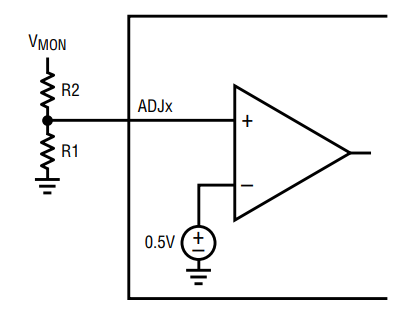
Figure 2. Monitoring a positive supply.
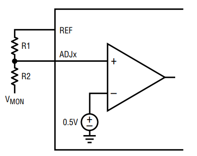
Figure 3. Monitoring a negative supply.
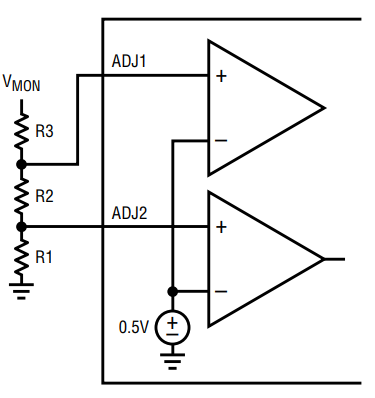
Figure 4. Monitoring a positive supply for UV and OV.
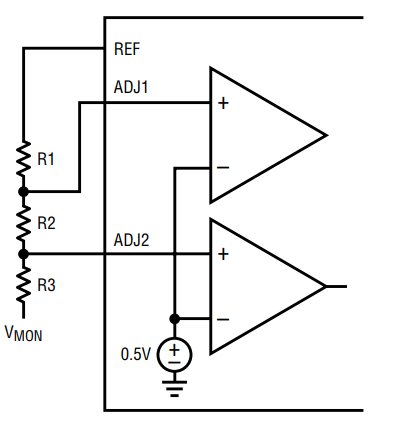
Figure 5. Monitoring a negative supply for UV and OV.
Selection of resistor values is driven by two factors: nominal trip point and current consumption. In particular, the selection of R1 is driven by current consumption, and the ratio of the other resistors to R1 determines the trip point. If the monitored voltage is typically close to its nominal trip threshold, the voltage across R1 is approximately 0.5V, so the current consumed by the resistor divider is about 0.5V/R1. Supplies that operate substantially away from their threshold cause the current consumption to deviate from the estimate above by about the same percentage by which they deviate from the threshold.
In most applications, the current consumption should be minimized. However, as the current is reduced, the impact of leakage at the tap point on the monitoring accuracy becomes more severe. The leakage current is drawn from the driving-point impedance at the ADJ input, so the fractional error is approximately:
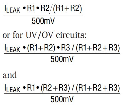
As a rule of thumb, the current in the divider should be at least 100 times the expected leakage, including the 15nA maximum internal to the part and any external leakage sources.
The rest of the resistor values are determined by the choice of trip point. Since the accuracy of the LTC2909 thresholds is guaranteed to 1.5% over the operating temperature and supply range, the trip points should usually be set 1.5% beyond the specified operating range of the monitored supply. For example, a 5V ±10% supply should have a 4.425V undervoltage trip point, not 4.5V. See the sidebar on threshold accuracy for an explanation.
Given a desired trip point, and the value of R1 chosen as above, it is then possible to calculate the appropriate values of the rest of the resistors. When monitoring a positive supply for a single fault condition, the user should choose

Similarly, for a negative supply (or positive supply with trip voltage below 0.5 V),

Note that if the desired trip voltage is below ground, the value VTRIP should be negative. The situation is slightly more complicated when only three resistors are used to monitor a single supply for UV and OV. For a positive supply with desired trip thresholds VTRIP(UV) and VTRIP(OV), the appropriate values are
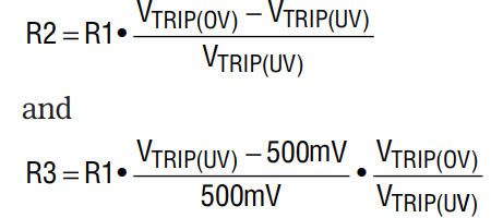
Finally, for a negative supply with desired trip thresholds VTRIP(UV) and VTRIP(OV), the appropriate values are:
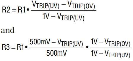
Tables 2 and 3 show suggested values of resistors for monitoring a number of standard supply voltages for UV, OV or UV and OV. Table 2 gives values for nominal supply accuracy of 5% (6.5% trip points), and Table 3 gives values for 10% supplies (11.5% trip points). In the tables, the values of R1 have been chosen to minimize the threshold error using standard 1% resistor values, while maintaining the divider current consumption near 5µA.
| Nominal Voltage |
5% UV |
5% OV |
5% UV and OV |
||||
| R1 | R2 | R1 | R2 | R1 | R2 | R3 | |
| 24 | 232k | 10.2M | 102k | 5.11M | 82.5k | 11.5k | 4.12M |
| 15 | 115k | 3.09M | 200k | 6.19M | 76.8k | 10.7k | 2.37M |
| 12 | 49.9k | 1.07M | 102k | 2.49M | 76.8k | 10.7k | 1.87M |
| 9 | 115k | 1.82M | 78.7k | 1.43M | 162k | 22.6k | 2.94M |
| 5 | 137k | 1.15M | 137k | 1.33M | 76.8k | 10.7k | 732k |
| 3.3 | 221k | 1.15M | 340k | 2.05M | 76.8k | 10.7k | 453k |
| 2.5 | 115k | 422k | 51.1k | 221k | 137k | 19.1k | 576k |
| 1.8 | 63.4k | 150k | 115k | 324k | 82.5k | 11.5k | 221k |
| 1.5 | 59.0k | 107k | 137k | 301k | 76.8k | 10.7k | 158k |
| 1.2 | 127k | 158k | 102k | 158k | 187k | 26.1k | 267k |
| 1.0 | 200k | 174k | 100k | 113k | 107k | 15.0k | 105k |
| –5 | 133k | 1.37M | 118k | 1.37M | 174k | 20.0K | 2.00M |
| –9 | 97.6k | 1.74M | 115k | 2.32M | 182k | 22.6k | 3.65M |
| –12 | 107k | 2.49M | 40.2k | 1.07M | 40.2k | 5.11k | 1.07M |
| –15 | 107k | 3.09M | 309k | 10.2M | 309k | 40.2k | 10.2M |
| Nominal Voltage |
10% UV |
10% OV |
10% UV and OV |
||||
| R1 | R2 | R1 | R2 | R1 | R2 | R3 | |
| 24 | 102k | 4.22M | 115k | 6.04M | 39.2k | 10.2k | 2.05M |
| 15 | 200k | 5.11M | 200k | 6.49M | 41.2k | 10.7k | 1.33M |
| 12 | 115k | 2.32M | 107k | 2.74M | 41.2k | 10.7k | 1.05M |
| 9 | 113k | 1.69M | 140k | 2.67M | 73.2k | 19.1k | 1.37M |
| 5 | 113k | 887k | 113k | 1.15M | 115k | 30.1k | 1.13M |
| 3.3 | 221k | 1.07M | 294k | 1.87M | 226k | 59.0k | 1.37M |
| 2.5 | 102k | 348k | 301k | 1.37M | 41.2k | 10.7k | 178k |
| 1.8 | 137k | 301k | 86.6k | 261k | 63.4k | 16.5k | 174k |
| 1.5 | 48.7k | 80.6k | 43.2k | 102k | 51.1k | 13.3k | 107k |
| 1.2 | 137k | 154k | 63.4k | 107k | 80.6k | 21.0k | 115k |
| 1.0 | 200k | 154k | 137k | 169k | 174k | 45.3k | 169k |
| –5 | 115k | 1.13M | 200k | 2.43M | 115k | 24.3k | 1.37M |
| –9 | 127k | 2.15M | 215k | 4.53M | 51.1k | 11.8k | 1.07M |
| –12 | 115k | 2.55M | 41.2k | 1.15M | 130k | 30.9k | 3.57M |
| –15 | 115k | 3.16M | 309k | 10.7M | 47.5k | 11.5k | 1.62M |
Why Is Threshold Accuracy Important?
In monitored systems, there is some voltage level beyond which the proper function of the devices connected to a supply bus cannot be guaranteed. Ideally, that is the voltage at which the supervisor should issue a reset, since this guarantees the proper function of the system while permitting the maximum allowable variation in supply voltage. Thus, in the ideal case, the power supply tolerance is as loose as the devices on the bus will tolerate.
Of course, any real supervisor has limited accuracy, which tightens the system constraints. Typically, monitor accuracy is specified as a percentage band around the nominal trip point in which the threshold is guaranteed to lie, such as ±1.5%. To prevent nuisance resets when the supply is operating normally, the supply tolerance and monitor accuracy bands should not overlap.
As an example, a supply with a specified tolerance of ±5%, monitored by a 1.5% accurate monitor must have its nominal threshold set at 6.5% to prevent nuisance resets. With that accuracy band, the supervisor is not guaranteed to issues a reset until the supply has reached the other end of the monitor accuracy band, at 8%. Therefore, the devices attached to the supply must function properly to at least an 8% deviation in supply voltage. If this is not possible, a supply with tighter tolerance must be provided. For comparison, if the 1.5% accurate supply monitor is replaced by a less accurate 2.5% device, the power supply tolerance must be tightened to ±3% to ensure the same 8% operation band, thus complicating the power supply design.
UVLO
The LTC2909 features a third high accuracy comparator on the VCC pin, which allows the part to function in some applications as a triple supply monitor. The polarity of the VCC comparator is fixed to be positive, so the comparator creates an accurate UVLO. The threshold of the UVLO is also fixed, and is set at 11.5% below the nominal threshold voltage specified in the part number. Versions are available for standard logic supplies: LTC2909-2.5 for 2.5V supplies (2.175V nominal threshold), LTC2909-3.3 for 3.3V supplies (2.921V nominal threshold), and LTC2909-5 for 5.0V supplies (4.425V nominal threshold). The LTC2909-2.5 is recommended for designs that do not want monitoring of the VCC pin. The UVLO then functions merely to ensure that RST is not allowed to go high while the VCC voltage is too low to guarantee proper accuracy of the ADJ input thresholds. The accuracy of the UVLO threshold is the same as the ADJ thresholds: ±1.5% guaranteed over the operating temperature range.
Glitch Immunity
A monitored supply generally has high frequency components riding on its DC value. These may be caused by load transients acting on non-zero output impedance (whether due to supply line impedance or regulation bandwidth), output ripple of the supply, coupling from nearby high-frequency signals, or noise. Ideally, the supply monitor should decide whether the supply voltage transient threatens the functionality of any of the devices which are powered by that voltage rail, and issue a reset if (and only if) it does. Unfortunately, a real supervisor cannot use an omniscient algorithm to know what exactly is connected to the bus or how those devices respond to supply transients. Given this, a number of possible approaches exist, addressing some of the concerns related to supply transients. These techniques focus on eliminating two undesirable situations that result from using a simple comparator.
One undesirable effect that must be prevented is rapid toggling of the reset output (“chattering”), caused by ripple, coupling, or noise on a supply voltage that is near the threshold. A common solution is to add hysteresis to the monitor threshold, which prevents chattering as long as the transient amplitude is less than the amount of hysteresis. Adding hysteresis effectively worsens the threshold accuracy, thereby unnecessarily reducing system uptime, or tightening the system requirements on supply voltage. For this reason, the LTC2909 uses other methods to prevent chattering, and does not have threshold hysteresis, unless the part is configured in comparator mode, where it would otherwise be more susceptible to chattering than usual (as explained below).
The primary defense against chattering is the programmed reset timeout period. If at any time during the reset timeout the supplies become invalid, the timer is immediately zeroed, and starts timing again from the beginning of the period when the supplies become valid again. Thus, any time the supply voltage is close enough to the threshold that the amplitude of the supply transients take the supply into the invalid region, RST remains low as long as the time between transients is less than the reset timeout. That is to say, the reset timeout prevents transients with frequency greater than 1/tRST from causing undesired toggling at the reset output. Because the timeout is defeated in comparator mode, the LTC2909 is free to chatter in that mode, so a small amount of one-sided hysteresis is added to the comparator thresholds. See “Timeout Control” below for a description of the hysteresis behavior.
The other concern that must be addressed is identifying which transients cause a problem for the devices on the supply bus. It can generally be assumed that those devices can continue to operate through short duration excursions outside the valid supply region, particularly because local decoupling capacitors help prevent such transients from appearing at the devices. If possible, the supervisor should not issue a reset during these conditions.
Consider, for example, what happens when a system spins up a hard drive connected to a monitored supply bus. The bus voltage briefly dips, possibly falling outside the valid region, and then returns, approximately, to its previous value. This is normal, expected behavior, and a microprocessor that is also connected to that bus should function normally through the transient (otherwise there is no way the system can ever safely use the hard drive). The supply monitor should not issue a reset to the microcontroller during such a transient.
To solve this problem, the LTC2909 has low-pass filtering on the comparator outputs, so that short duration glitches on the monitored supply are not passed through to the control logic. For most systems, the response of the system to a glitch depends on the energy contained in the glitch, rather than just the voltage amplitude of the glitch. The duration of the glitch also factors into that energy, so the probability of a failure increases as the duration of the glitch increases (e.g. a 20% glitch on the supply may only be tolerable for 100µs, whereas a 5% glitch is tolerable for 1ms). The filtering on the LTC2909 comparators reflects this tendency. Figure 6 shows a typical curve of the maximum glitch duration that does not result in the LTC2909 issuing a reset, versus the percentage amount the glitch goes into the invalid region.
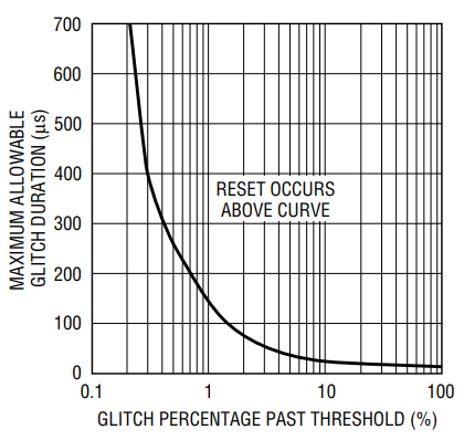
Figure 6. Allowable glitch duration as a function of magnitude.
Some of these concerns can be exacerbated by circuit board layout, so it is also important that some care be taken in the layout near the LTC2909. In applications which use negative polarity comparators, capacitive coupling from the RST output to the negative-polarity input can cause the part to oscillate at approximately 1/tRST if the negative-polarity input is sufficiently close to threshold: the capacitive coupling creates AC negative feedback around the part. To prevent this oscillation, the RST line should be kept away from the relevant ADJ inputs, and, where possible, from the corresponding supply. Negative-polarity applications may also oscillate when the RST is driving a large load, which causes a voltage difference between the ground of the 0.5V internal reference, and the ground of the monitored voltage. Several factors can help eliminate this source of oscillation. First and foremost, the current sunk by RST should be kept below 1mA if possible. Good grounding practice is also important. Input resistor dividers which connect to ground should have a Kelvin-sense trace directly to the GND pin, and the path from the monitored supply ground to the GND pin should be low impedance (preferably through a good ground plane).
Timeout Control
As described above, the LTC2909 has a reset timeout delay which helps reduce the sensitivity of the monitor to supply glitches. For convenience, this reset timeout can be controlled in three different ways. If a 200ms timeout is appropriate for the application (based on expected noise distributions and system timing specifications), no external components are needed to set the timeout—simply tie the TMR pin to ground, and the LTC2909 uses an internal 200ms delay generator.
For applications that require timeout periods other than 200ms, the delay can be set by connecting the TMR pin to a grounded capacitor, where the delay is set at approximately 9ms per nF of capacitance. To ensure timer accuracy, the timing capacitor should be a low leakage ceramic type. Leakage currents over 500nA substantially impair timer function. As an example, for a 50ms delay, the timer capacitor should be 50/9 = 5.6nF.
Figure 7 shows the typical timeout period as a function of the capacitor on the TMR pin. Due to inherent capacitance on the TMR pin, the minimum attainable timeout period in external mode is about 400µs, with no external capacitor connected to the pin. The maximum timeout is limited to nine seconds (1µF capacitor) by startup concerns. Assuming that the timer capacitor is initially discharged during the power-up sequence, the LTC2909 initially sees that the TMR voltage is near ground, and thus operates in internal timeout mode. As soon as the part is powered, a 2µA current source begins pulling up on the TMR pin, charging the timer capacitor towards the ground sense threshold (approximately 250mV). If all three supply inputs (VCC and both ADJ inputs) become valid, and the 200ms internal timeout period completes before the TMR voltage reaches the ground sense threshold, RST goes high after a much shorter delay than was intended. If this startup behavior is not a problem in a given system, the maximum timeout is limited only by the availability of large capacitors with leakage currents below 500nA.
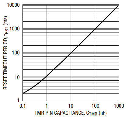
Figure 7. Reset timeout period as a function of capacitance.
Finally, there are some systems where the reset timeout delay is undesirable. For example, this may be the case in applications where the user is not using the LTC2909 RST pin as a system reset line. If the user ties the TMR pin to VCC, the LTC2909 is put into comparator mode. In comparator mode, the timeout delay is bypassed, and the comparator outputs are connected directly to the RST drive circuitry. Due to the glitch-rejecting low-pass filter in the comparators, there will still be some delay from the inputs to the RST output, based on the amount of overdrive on the input. As shown by Figure 6, the propagation delay for large overdrives is about 25µs.
In comparator mode, because the reset timeout has been removed, the glitch and oscillation immunity of the part have been decreased. To prevent undesired “chattering” of the RST output when the input voltages are very close to threshold, a small amount of one-sided hysteresis is added to all three comparators. The hysteresis is “one-sided” in the sense that the valid-to-invalid transition is unaffected, but the invalid-to-valid threshold is moved about 0.7% into the valid region. Thus, for the ADJ inputs, the threshold voltages in comparator mode are a function of the SEL pin state. Nominal values are shown in Table 4.
| Input |
SEL = GND | SEL Open | SEL = VCC | |
| ADJ1 |
Rising | 500.0mV | 503.5mV | 503.5mV |
| Falling | 496.5mV | 500.0mV | 500.0mV | |
| ADJ2 |
Rising | 500.0mV | 500.0mV | 503.5mV |
| Falling | 496.5mV | 496.5mV | 500.0mV | |
Shunt Regulator
In most systems, it is possible to identify one supply as the one with highest availability—that is to say the supply which is most likely to be on, first to power up, last to shut down, and so on. There are a number of advantages to powering a supply supervisor from this highest-availability supply. First, the RST pull-down circuits are powered by the part supply. Thus, having the part supply come up first helps guarantee that RST never floats high due to insufficient pull-down strength. Conversely, powering the part from a high-availability supply helps maximize the up-time of the system because the LTC2909 will not release the RST output unless the part is properly powered.
The problem in many systems is that the high-availability supply is also a relatively high-voltage supply. For example, the highest availability supply in an automotive system is the 12V (nominal) battery voltage, and in a telecom system it is likely to be a 48V supply. Most supply supervisors require an external voltage regulator to operate from these supplies, but the LTC2909 saves components by integrating a 6.5V shunt regulator into the VCC pin. All that is required is a series-dropping resistor between the high-voltage supply and the VCC pin. This scheme allows the LTC2909 to be powered from an arbitrarily high voltage, subject only to constraint by the power dissipation in the shunt resistor. Furthermore, the VCC pin can be used to power other low voltage parts, as long as their supply current (which should be less than 5mA) is factored into the selection of the resistor.
The shunt regulation voltage is nominally 6.5V, and is guaranteed to lie between 6.0V and 6.9V across the entire operating temperature range and across a wide range of shunt current. Selection of the series resistor is driven by the shunt regulator bias current. The shunt regulator bias will be set by the amount of current flowing through the resistor (based on its value and the voltage drop across it), minus the supply current of the part, including any load drawn from the REF pin, and the load currents of any other devices that take advantage of the 6.5V supply at the VCC pin. The series resistor should be chosen to bias the shunt regulator somewhere between 50µA and 10mA, ideally around 1mA.
These design constraints impose the following limits on the series resistor. The maximum load drawn from the reference, plus the maximum load drawn by other devices connected to the VCC pin, plus 150µA for the LTC2909 must be less than the minimum current through the resistor by at least 50µA:

This ensures that the shunt regulator is biased with at least 50µA of current. On the other side, the minimum load on the reference, plus the minimum load drawn by other devices on VCC must be less than the maximum current through the resistor by at most 10mA:
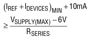
This ensures that the regulator is never shunting more than 10mA of current. In summary, the series resistor is required to satisfy:
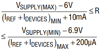
As an example, consider operation from an automobile battery. For purposes of this example, the operating range of the battery supply is approximately 10V to 60V, and we can suppose that the user’s loading of REF and external current use can each range from 0µA to 100µA. The minimum value of R is then 54V/10mA = 5.4k, and the maximum is 3.1V/400µA = 7.75k. Given these constraints, a value of 6.8k is probably optimal.
The above equation is actually overly restrictive. In cases where the supply voltage is very close to the shunt regulation voltage, it may be impossible to satisfy the above equation because the maximum allowable value is less than the minimum. In these cases, it may be assumed that the maximum allowable value is 1k instead of the value predicted by the formula above, as long as the VCC pin is not used to power other devices. There are scenarios where the shunt regulator cannot satisfy the needs for VCC (e.g. those with a very large possible supply range). These applications must use an external voltage regulator of some sort, which, of course, should have a regulation voltage below 6V.
A final consideration is the power dissipation in the series resistor, which may be quite high for high voltage supplies. The series resistor must be rated to handle a power of at least

A rough rule of thumb suitable for many applications (those that have fairly constant REF current draw, and have minimum supply voltages well above 6V) is that the resistor rating should be at least 0.1 Watt per 100 volts of maximum supply, multiplied by the ratio of maximum to minimum supply voltage.
Returning to the automobile battery example from above, the power dissipated in the 6.8k resistor could be as large as 542/6800 = 0.43W (the rule of thumb would give 0.36W), so a 0.5W resistor is best. In reality, of course, the battery is unlikely to stay at 60V for long enough to heat up the resistor substantially. If we were to take a more reasonable DC maximum of 16V, the resistor only needs to handle about 15mW.
Applications
±12V UV Monitor with Manual Reset
Figure 8 shows a LTC2909 configured as an undervoltage monitor for a system with ±12V supplies, and a 1.8V logic bus. The part is powered from the high-availability 12V supply through the series dropping resistor RCC. The floating condition of SEL sets the polarity for one positive and one negative UV. The reset timeout is set to 20ms nominal by CTMR, which allows faster recovery from faults. Finally, the pushbutton allows the user to drive ADJ1 to ground, manually forcing a reset condition. The release of the pushbutton is debounced by the LTC2909’s reset timeout. If ESD from people touching the pushbutton is a concern, a 10k resistor in series with the pushbutton limits the current flow into the LTC2909 to prevent damage.
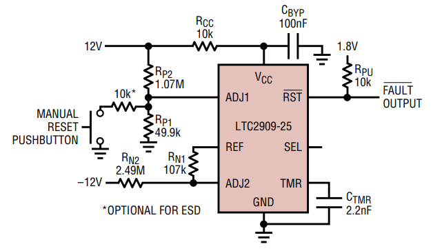
Figure 8. ±12V undervoltage monitor with pushbutton reset.
48V Telecom UV/OV Monitor with Hysteresis
Telecom supply specifications usually require some amount of hysteresis in the acceptable voltage range. Since the LTC2909 does not generally have hysteresis in its thresholds, the hysteresis must be externally added. Figure 9 shows the LTC2909 configured to monitor a 48V nominal supply bus for UV and OV. The NMOS devices lower the UV threshold (by reducing R2 for ADJ1) and raise the OV threshold (by reducing R1 for ADJ2) while the RST is high. This has the effect of widening the acceptable supply window once the supply becomes good. The resistors are chosen so that the window is 43.3V–70.2V when the supply is outside the window, and 38.7V–71.6V once the supply is good. Since the part is powered from the 48V bus, the series-dropping resistor is required to be a 0.25W device to handle the power dissipated when the bus is overvoltage.
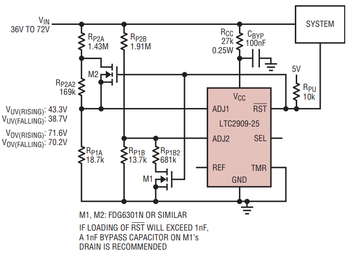
Figure 9. A 48V telecom UV/OV monitor with hysteresis.
The recommended NMOS device is FDG6301N, which combines both NMOS devices in one SC70-6 package. Other devices may be used as long as the threshold voltage is guaranteed to be much less than 5V, and the drain-source breakdown is greater than 10V. Note that if the RST output is loaded with a large capacitance, the feedback through the gate-drain capacitance of M1 can cause the circuit to oscillate unless a bypass capacitor is placed on M1’s drain.
Automotive Supply System
Figure 10 shows three LTC2909s in a full-featured automotive supply system, providing overvoltage, overcurrent, and over-temperature protection in addition to an undervoltage system reset. The system uses an LT1641-2 Hot Swap controller as a controlled electronic circuit breaker. The IRLZ34 logic-NFET serves as the disconnect switch, and the 10mΩ sense resistor sets a current limit of 4.7A. After an over-current fault, the LT1641-2 reconnects after a delay of 160ms (set by CT).
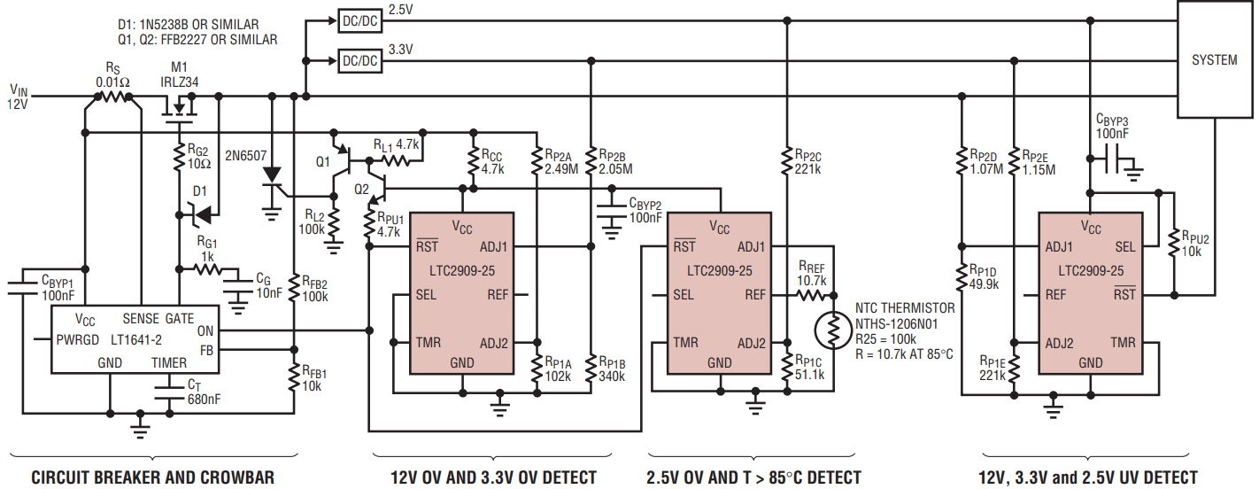
Figure 10. Automotive supply system with overvoltage, overcurrent and overtemperature protection.
The two LTC2909s on the left are responsible for detecting overvoltage and over-temperature conditions. To guarantee that they function properly, they must be powered from the 12V input. The VCC pins are tied together, and the supply current flows through just one dropping resistor, so the voltage tends to regulate at whichever of the shunt regulation voltages is the lower of the two.
When any of the supply voltages goes overvoltage, or the temperature sensor is heated above 85°C, the shared RST line is pulled low by one of the two LTC2909s. This takes the LT1641-2 ON input low, disconnecting the power switch. At the same time, current is pulled through Q2, turning on Q1, which triggers the 2N6507 SCR and thereby crowbars the 12V supply to the system, removing the overvoltage condition. After the fault condition disappears, the LTC2909s apply a 200ms timeout before reconnecting to the 12V input.
The third LTC2909 serves to provide a master reset to the system when any of the three supplies are undervoltage, whether because insufficient input voltage is present, or because one of the protection faults has tripped. The third monitor function is provided by the UVLO.
A Dale NTHS-1206N01 NTC thermistor with room temperature resistance of 100k is used to detect the temperature, and may be physically located wherever temperature monitoring is needed. The thermistor forms part of a resistor divider from the buffered reference output to ground. As long as the temperature is below 85°C, the thermistor resistance is greater than RREF, so ADJ1 is above its threshold, and RST is allowed to go high. If the temperature rises, the thermistor resistance decreases, pulling down on ADJ1, and causing a reset when its resistance is equal to or lower than RREF.
Conclusion
The LTC2909 is a true one-size-fits-all power supply monitor—a way to simplify design and parts stock. It provides a compact solution to monitoring any two supplies for almost any fault condition, where input polarity selection and a buffered reference output allow monitoring of OV conditions and negative supplies. Precision comparators, including a third input on the part’s VCC, increase system reliability. To simplify design further, no regulated voltage is required—a built-in shunt regulator on VCC allows operation from a high-voltage high-availability supply. An accurate model of the LTC2909 is included with SwitcherCAD (available at www.analog.com), as an aid to rapid development.

