Complete 3-Rail Power Supply in a 4mm × 4mm QFN Package
Introduction
Battery-powered portable electronic devices such as portable media players, handheld PCs, and GPS receivers typically require several internal power supply rails: a 3.0V or 3.3V supply for audio, motor drivers, and micro hard disk drives; a 1.2V or 1.5V rail for a logic core; and often a 1.8V supply to support Flash memory. For devices supplied by a Li-Ion battery, the power system is further complicated by the fact that the 3.0/3.3V output rail lies within the discharge voltage range of the battery, thereby mandating a power supply solution that can step the input voltage up or down depending on the battery's state of charge. In addition, most systems require specific power-up sequencing between the multiple output voltage rails to ensure consistent and reliable system initialization.
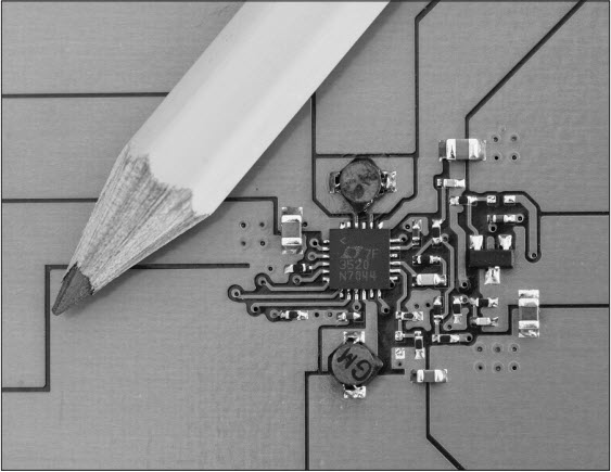
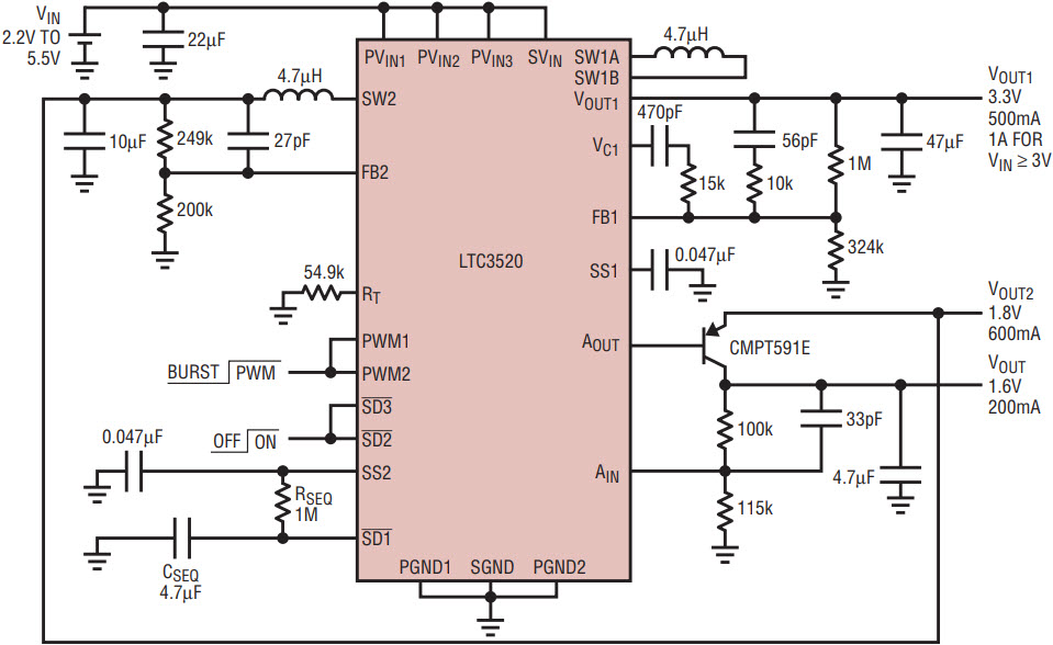
Figures 1 and 2 show how all of these requirements can be met with a single tiny IC and relatively few additional components. The heart of this complete power supply system is the LTC3520, which includes a high-efficiency, internal 1A buck-boost converter, a 600mA synchronous buck converter and an LDO controller, all in a 4mm × 4mm QFN package.

Figure 1. Complete triple-output supply: Li-Ion to 3.3V, 1.8V, and 1.5V.

Figure 2. Sequenced start-up, triple-output converter.
The LTC3520’s buck-boost converter utilizes an advanced switching algorithm to precisely regulate the output voltage with input voltages that are above, below, or even equal to the output voltage. Mode transitions occur seamlessly and high efficiency and low noise performance are maintained across all operational modes. The synchronous buck converter operates with current-mode control and is internally compensated to reduce the number of external components. If the input voltage falls below the minimum buck regulation voltage, the buck converter automatically transitions to low dropout mode to extend battery life. Pin-selectable Burst Mode® operation improves light-load efficiency and reduces the no-load input current for both converters to only 70µA.
The extensive array of programmable features on the LTC3520 provide the flexibility needed to meet the requirements of a wide range of applications. Both the buck and buck-boost converters are controlled by a common oscillator. A single external resistor sets the switching frequency, making it possible to optimize efficiency and application size. Both converters feature voltage mode soft-start with ramp rates which are independently set via small external capacitors. The output voltage of each converter is programmed via an external resistor divider. The buck-boost output voltage can be set as high as 5.25V or as low as 2.2V. When configured for a 3.3V output, the buck-boost can provide up to 1A load current for input voltages greater than 3V and supports a 500mA load down to an input voltage of 2.2V. The buck converter delivers up to 600mA and its output can be set as low as 0.8V.
Three Output Rails with Sequenced Start-Up
In many applications, the low voltage rails that supply the logic core and memory must be powered and in regulation before the higher voltage supply for the peripheral devices is activated. This provides time for the processor to initialize and control the states of its logic outputs to ensure reliable and consistent initialization of the system. Figure 2 shows power-up sequencing achieved by using the buck converter soft-start pin to enable the buck-boost via the SD1 pin after a programmable delay created by the RC filter composed of resistor RSEQ and capacitor CSEQ.
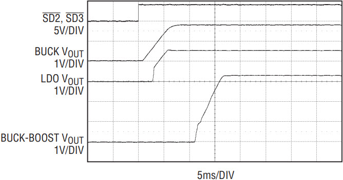
Figure 3 shows the output voltages for this application circuit during start-up. The buck output voltage begins its soft-start period soon after the rising edge of SD2 and the LDO output rises coincident with the buck output. Approximately 5ms after the buck reaches regulation, the buck-boost soft-start commences. The length of this delay can be adjusted via the time constant of the RC filter, while the ramp rate of each converter's soft-start can be independently controlled by the value of the respective soft-start capacitor. In shutdown, SD2 is held low, which internally forces SS2 low, thereby ensuring the buck-boost converter remains disabled as well.

Figure 3. Output voltages during sequenced start-up.
Low Battery and Power-Good Detection
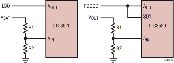
In applications where the third output rail is not required, the LDO controller can be used instead as a general purpose comparator. One possibility is to utilize the uncommitted amplifier as a low battery indicator with the circuit shown in Figure 4a. The low battery output can then be used to provide the system processor with feedback on the state of the battery. The uncommitted amplifier is not disabled by the undervoltage lockout, which allows the low-battery indicator to remain functional down to 1.6V typically, well below the undervoltage lockout threshold of the LTC3520.

Figure 4. Implementation of low battery and power-good indicators.
It is also possible to use the uncommitted amplifier as a high accuracy power-good indicator for either the buck or buck-boost output rail. The resultant power-good signal can then be utilized to enable the opposite channel, providing high accuracy supply sequencing. For example, the circuit shown in Figure 4b creates a power-good output for the buck converter and initiates the buck-boost converter only after the buck output reaches the power-good threshold set by resistors R1 and R2.
USB-Powered Triple-Output Supply
The USB specification mandates that the output voltage provided by a high power port be maintained in the range of 4.75 to 5.25V. However, once resistive drops in the USB cable and connectors are taken into account, along with the potential voltage drop across an upstream bus-powered hub, a USB peripheral must be able to function with input voltages over a wider range of 4.25 to 5.25V. Furthermore, the input voltage seen by the peripheral can vary dynamically between these limits based on the particular cable, host, and load current being drawn. In such applications, the buck-boost converter of the LTC3520 can provide a restored 5V output rail independent of loading and cable resistance. Additionally, the buck converter and LDO can be configured to provide two lower voltage outputs, such as 3.3V and 1.8V logic supplies. If both of these additional voltage outputs are not required, the uncommitted amplifier can instead be configured to monitor the input USB voltage to inform the processor of the presence of a valid USB input voltage level.
Conclusion
With its small size, flexible programmability, and high efficiency, the LTC3520 is well suited to meet the multiple output power supply needs of most Li-Ion powered electronic devices. In addition, the LTC3520 is ideal for systems powered from USB or low voltage wall adapters, which require an output voltage rail that lies within the expected input voltage range due to resistive drops in the supply path.


