
MAXREFDES1176


製品概要
設計リソース
説明
Power over Ethernet (PoE) is a technology that allows network cables to deliver power to a powered device (PD) through power-sourcing equipment (PSE) or midspan, and has many advantages over traditional methods of delivering power. PoE allows power and data to be combined, removing the need for altering the AC mains infrastructure and can be installed by non-electricians. PoE is an intelligent system designed with protection at the forefront, preventing overload, underpowering, and installation errors, while allowing simple scalability and reliability.
The MAX17690 eliminates the need for an optocoupler or auxiliary transformer winding and achieves ±5% output voltage regulation over line, load, and temperature variations. The MAX17690 implements an innovative algorithm to accurately determine the output voltage by sensing the reflected voltage across the primary winding during the flyback time interval. By sampling and regulating this reflected voltage when the secondary current is close to zero, the effects of secondary-side DC losses in the transformer winding, the PCB tracks, and the rectifying diode on output voltage regulation can be minimized.
The MAX17690 also compensates for the negative temperature coefficient of the rectifying diode.
機能と利点
- IEEE® 802.3af/at Compliance
- Thermally Enhanced, 3mm × 3mm, 10-Pin TDFN Package (MAX5969B)
- 30V to 60V Input Voltage Range
- Programmable Switching Frequency from 50kHz to 250kHz
- Programmable Input Enable/UVLO Feature
- Programmable Input Overvoltage Protection
- Adjustable Soft-Start
- 2A/4A Peak Source/Sink Gate Drive Capability
- Hiccup Mode Short-Circuit Protection
- Fast Cycle-by-Cycle Peak Current Limit
- Thermal Shutdown Protection
- Space-Saving, 16-Pin, 3mm x 3mm TQFN Package
- -40°C to +125°C Operating Temperature Range
詳細
Power over Ethernet (PoE) is a technology that allows network cables to deliver power to a powered device (PD) through power-sourcing equipment (PSE) or midspan, and has many advantages over traditional methods of delivering power. PoE allows power and data to be combined, removing the need for altering the AC mains infrastructure and can be installed by non-electricians. PoE is an intelligent system designed with protection at the forefront, preventing overload, underpowering, and installation errors, while allowing simple scalability and reliability.
The MAX17690 eliminates the need for an optocoupler or auxiliary transformer winding and achieves ±5% output voltage regulation over line, load, and temperature variations. The MAX17690 implements an innovative algorithm to accurately determine the output voltage by sensing the reflected voltage across the primary winding during the flyback time interval. By sampling and regulating this reflected voltage when the secondary current is close to zero, the effects of secondary-side DC losses in the transformer winding, the PCB tracks, and the rectifying diode on output voltage regulation can be minimized.
The MAX17690 also compensates for the negative temperature coefficient of the rectifying diode.
Other features include the following:
- IEEE® 802.3af/at Compliance
- Thermally Enhanced, 3mm × 3mm, 10-Pin TDFN Package (MAX5969B)
- 30V to 60V Input Voltage Range
- Programmable Switching Frequency from 50kHz to 250kHz
- Programmable Input Enable/UVLO Feature
- Programmable Input Overvoltage Protection
- Adjustable Soft-Start
- 2A/4A Peak Source/Sink Gate Drive Capability
- Hiccup Mode Short-Circuit Protection
- Fast Cycle-by-Cycle Peak Current Limit
- Thermal Shutdown Protection
- Space-Saving, 16-Pin, 3mm x 3mm TQFN Package
- -40°C to +125°C Operating Temperature Range
This reference circuit consists of the MAX5969B PD controller and an isolated no-opto flyback DC-DC converter using the MAX17690 and MAX17606 to demonstrate a 5V DC output application. A 1GbE RJ45 magnetic jack is also included as well as two diode bridges for separating data and DC power provided by an endspan or midspan PoE system. The low-resistance, on-chip MOSFETs ensure high efficiency at full load and simplifies layout. The power supply delivers up to 1.4A at 5V. Table 1 shows an overview of the design specification.
| Parameter | Symbol | Min | Max |
| Input Voltage | VIN | 30V | 60V |
| Power Range | PIN | 6.49W | 12.95W |
| Undervoltage Lockout Voltage | VUVLO | 29.4V | |
| Frequency | fSW | 143.3kHz | |
| Peak Efficiency at Full Load | ηMAX | 90% | |
| Efficiency at Minimum Load | ηMIN | 61% | |
| Output Voltage | VOUT | 5V | |
| Output Voltage Ripple | ∆VO | 50mV | |
| Maximum Output Current | IOUT | 1.4A | |
| Maximum Output Power | POUT | 7W | |
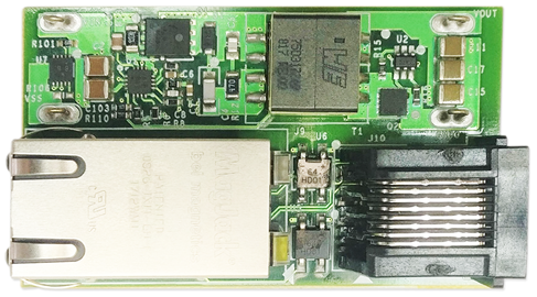
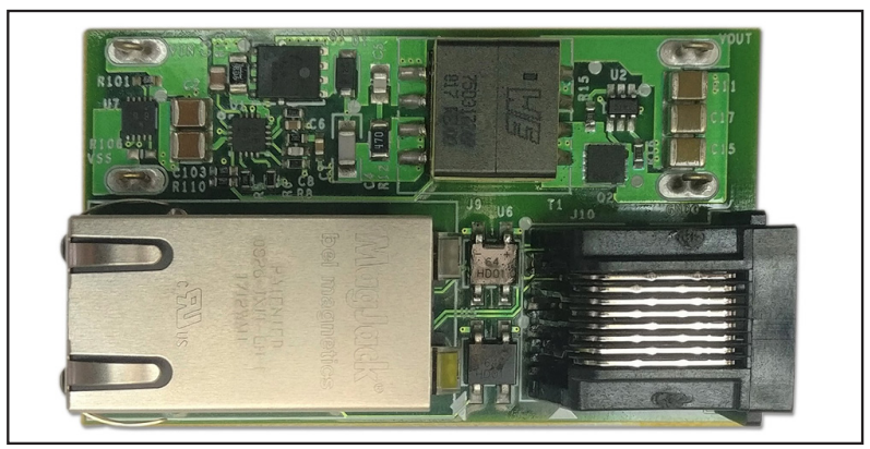
This document describes the hardware shown in Figure 1. It provides a detailed technical guide to designing a complete interface for a PD to comply with the IEEE 802.3af/at standard in a PoE class 3 system and an isolated no-opto flyback DC-DC converter using the MAX17690 controller and MAX17606 secondary-side synchronous MOSFET driver. The power supply has been built and tested.
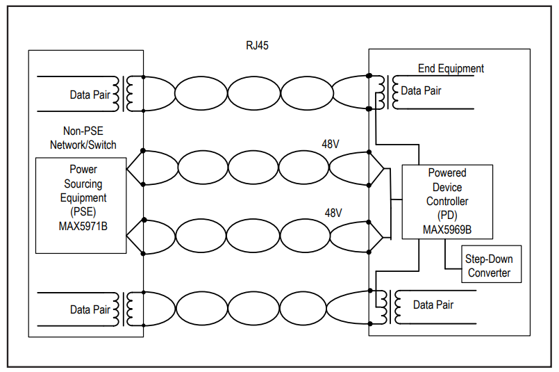
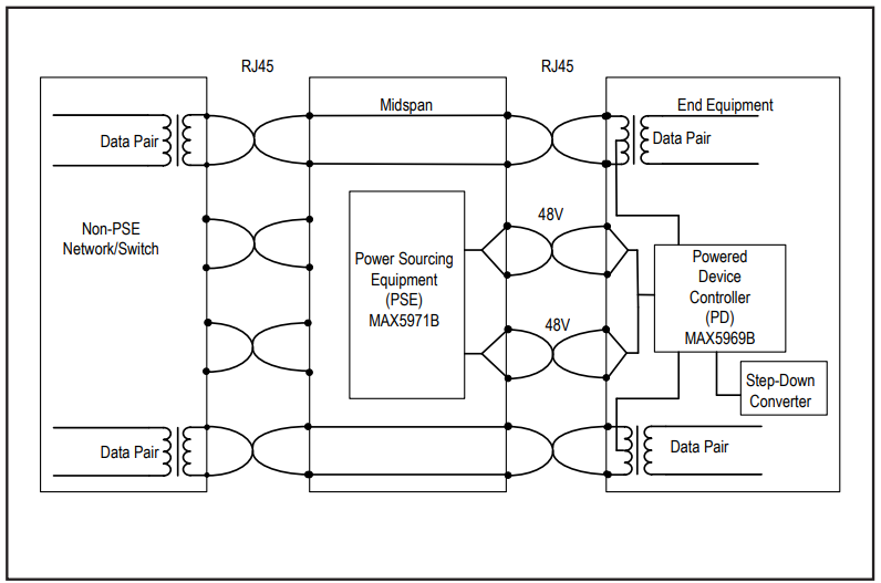
A PoE system delivers power and data to an end device (PD) typically through an RJ45 cable power from an endspan (PSE) (Figure 2) or a midspan (Figure 3). The power is separated from the data through diode bridges to deliver a typical 48V for efficient power transfer, which is low enough to be considered a safe voltage, and removes the need to rewire AC mains and saves cost.
Although this voltage is safe for humans, it still can damage equipment if not properly delivered. This is where MAX5969B classification is required, ensuring the equipment can handle the power delivery. Before the PSE can enable power to a connected IP camera or other PD, it must perform a signature detection.
Signature Detection
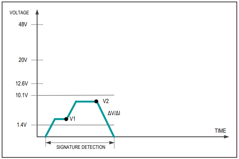
Signature detection uses a lower voltage to detect a characteristic signature of IEEE-compatible PDs (a 24.9kΩ resistance). See Figure 4. Once this signature has been detected, the PSE knows that higher voltages can be safely applied. The PSE applies two voltages on VIN in the range of 1.4V to 10.1V (1V step minimum) and then records the current measurements at the two applied voltages. The PSE then computes the change in current when each voltage was applied (ΔV/ΔI) to ensure the presence of the 24.9kΩ signature resistor.
Classification
In classification mode, the PSE classifies the PD based on the power consumption required. (The IEEE 802.3af/ at standard defines only class 0 to 4 and class 5 for any special requirement.)
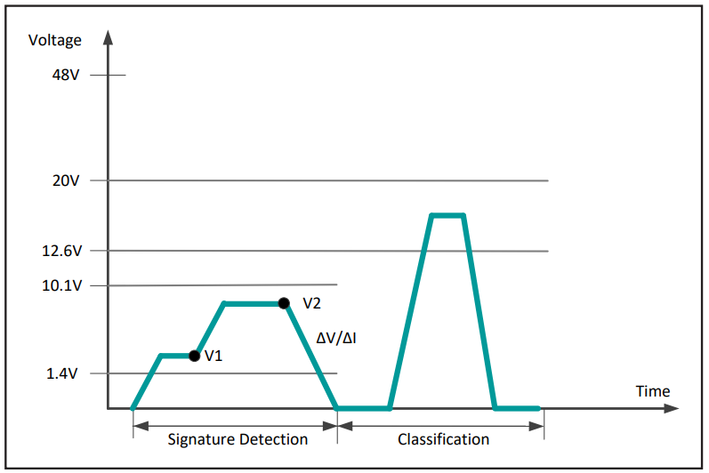
An external resistor (RCLS) of 43.7Ω connected from CLS to VSS sets the classification current. The PSE determines the class of a PD by applying a voltage at the PD input and measuring the current sourced from the PSE.
When the PSE applies a voltage between 12.6V and 20V, the MAX5969A/MAX5969B exhibit a current of 26mA to 30mA. The PSE uses the classification current information to classify the power requirement of the PD (MAX5969B).
The classification current includes the current drawn by RCLS and the supply current of the MAX5969A/MAX5969B so the total current drawn by the PD is within the IEEE 802.3af/at standard figures. The classification current is turned off whenever the device is in power mode (Figure 5).
Power Mode
The final stage after detection and classification of a newly connected PD is to enable power. The 48V supply from the PSE is connected to the PD through the RJ45 cable. Once enabled, the PSE continues to monitor the amount of current being delivered to the PD and cuts power to the cable if the power drawn is not within the correct range. This protects the PSE against overload, underpowering and ensuring that the PSE is disconnected from the cable if the PD is unplugged or faulted. See Figure 6.
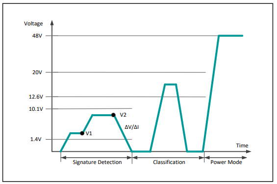
The MAX5969B enters power mode when VIN rises above the undervoltage lockout threshold (VON). Note that VON/VOFF = 38.6V/31V for the MAX5969B. When VIN rises above VON, the MAX5969B turns on the internal n-channel isolation MOSFET to connect GND to RTN. The open-drain power-good output (PG) remains low for a minimum of tDELAY until the power MOSFET fully turns on to keep the downstream DC-DC converter disabled during inrush. The PGOOD open-drain output is also connected to three small-signal transistors to prevent the DC converters from powering up before the power from the PD is allowable.
| Class | Maximum Power Used by PD (W) | RCLS (Ω) | VIN* (V) | Class Current Seen at VIN (mA) | IEEE 802.3af/at PSE Classification Current Specification (mA) | ||
| Min | Max | Min | Max | ||||
| 0 | 0.44 to 12.95 | 619 | 12.6 to 20 | 0 | 4 | 0 | 5 |
| 1 | 0.44 to 3.94 | 117 | 12.6 to 20 | 9 | 12 | 8 | 13 |
| 2 | 3.84 to 6.49 | 66.5 | 12.6 to 20 | 17 | 20 | 16 | 21 |
| 3 | 6.49 to 12.95 | 43.7 | 12.6 to 20 | 26 | 30 | 25 | 31 |
| 4 | 12.95 to 25.5 | 30.9 | 12.6 to 20 | 36 | 44 | 35 | 45 |
| 5 | > 25.5 | 21.3 | 12.6 to 20 | 52 | 64 | — | — |
*VIN is measured across the MAX5969A/MAX5969B input VDD to VSS.
Place the input capacitor, classification resistor, and transient voltage suppressor as close as possible to the MAX5969A/MAX5969B. Use large SMT component pads for power dissipating devices such as the MAX5969A/MAX5969B and the external diodes. Use short and wide traces for high-power paths.
The MAX5969B enters undervoltage lockout when the input voltage drops below 31V. When the input drops below this value, the isolation MOSFET switches off, disconnecting the 48V from the buck converters. The MAX5969B exits undervoltage lockout when the input exceeds 38.6V.
関連資料
-
MAXREFDES1176 Design FIles2021/03/03ZIP3 M
サポートおよびトレーニング
技術的なご質問についての回答は、ナレッジベースを検索してください。また、アナログ・デバイセズのアプリケーション・エンジニアの専任チームが、技術的なご質問にお答えいたします。