
製品概要
設計リソース
デバイス・ドライバ
コンポーネントのデジタル・インターフェースとを介して通信するために使用されるCコードやFPGAコードなどのソフトウェアです。
説明
The MAXREFDES1154 is a configurable 4-channel RTD/ TC measurement system. Each channel can be configured as either RTD input or TC input using RTD for cold junction compensation. The RTD can either be PT100 or PT1000 connected in 2-wire or 3-wire configuration. The same configuration can also be used to measure resistance. MAXREFDES1154 also supports all types of thermocouples, using RTD for cold junction compensation, which can be PT100 or PT1000, but it needs to be configured as a 2-wire connection.
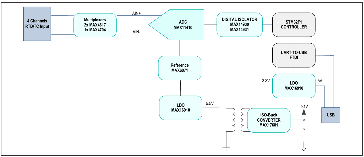
The MAXREFDES1154 provides a complete system solution for highly accurate temperature measurement in industrial applications. Analog front end includes two 8:1 multiplexer MAX4617 and one 4:1 multiplexer MAX4704 for RTD/TC input selection, and one 24-bit, 10-channel ADC MAX11410.
The microcontroller on board is used to communicate with the MAX11410 ADC, control the multiplexers, and process the ADC conversion results. The 24V field input power supply is isolated from both the analog front end and the microcontroller, which is powered using a USB. Isolation enhances system robustness, an important consideration in harsh industrial applications.
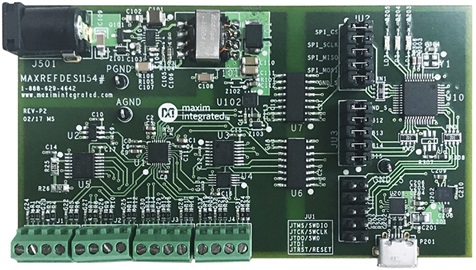
The MAXREFDES1154 design integrates two 8:1 multiplexer (MAX4617) and one 4:1 multiplexer (MAX4704), a 24-bit 10-channel ADC with internal PGA buffers (MAX11410), a high-precision 1.250V voltage reference (MAX6071), 2.75kVRMS digital isolator (MAX14930 and MAX14931), a STM32F1 microcontroller, a μP supervisor (MAX6730), a FTDI USB-UART bridge, a high-efficiency Iso-Buck DC-DC converter (MAX17681), and an isolated/regulated +3.3V power rail (MAX16910). The entire system typically consumes less than 300mW and fits onto a 5cm x 9cm board. It is targeted for industrial PLC applications.
機能と利点
- Highly accurate measurement
- Four channels
- Each channel can be configured as either RTD or TC input
- Supports 2-wire and 3-wire RTD
- Supports all types of thermocouple
- Thermocouple with RTD for cold junction compensation
- Sensor open detection
- 24V input protection
- Isolated power and data
- Board-level calibration
詳細
The MAXREFDES1154 is a configurable 4-channel RTD/TC measurement system. Each channel can be configured as either RTD input or TC input using RTD for cold junction compensation. The RTD can either be PT100 or PT1000 connected in 2-wire or 3-wire configuration. The same configuration can also be used to measure resistance. MAXREFDES1154 also supports all types of thermocouples, using RTD for cold junction compensation, which can be PT100 or PT1000, but it needs to be configured as a 2-wire connection.
The MAXREFDES1154 provides a complete system solution for highly accurate temperature measurement in industrial applications. Analog front end includes two 8:1 multiplexer MAX4617 and one 4:1 multiplexer MAX4704 for RTD/TC input selection, and one 24-bit, 10-channel ADC MAX11410.
The microcontroller on board is used to communicate with the MAX11410 ADC, control the multiplexers, and process the ADC conversion results. The 24V field input power supply is isolated from both the analog front end and the microcontroller, which is powered using a USB. Isolation enhances system robustness, an important consideration in harsh industrial applications.
The MAXREFDES1154 design integrates two 8:1 multiplex er (MAX4617) and one 4:1 multiplexer (MAX4704), a 24-bit 10-channel ADC with internal PGA buffers (MAX11410), a high-precision 1.250V voltage reference (MAX6071), 2.75kVRMS digital isolator (MAX14930 and MAX14931), a STM32F1 microcontroller, a µP supervisor (MAX6730), a FTDI USB-UART bridge, a high-efficiency Iso-Buck DC-DC converter (MAX17681), and an isolated/regulated +3.3V power rail (MAX16910). The entire system typically consumes less than 300mW and fits onto a 5cm x 9cm board. It is targeted for industrial PLC applications.
Other features include:
- Highly accurate measurement
- Four channels
- Each channel can be configured as either RTD or TC input
- Supports 2-wire and 3-wire RTD
- Supports all types of thermocouple
- Thermocouple with RTD for cold junction compensation
- Sensor open detection
- 24V input protection
- Isolated power and data
- Board-level calibration
The MAXREFDES1154 features four channels of RTD or TC input, supports PT100 or PT1000, and all types of thermocouple. Power and data are isolated. MAXREFDES1154 includes the following major components: isolated power supply, analog front end, ADC, and microcontroller.
The isolated power supply generates the power rails necessary for the analog front end and ADC from the 24V input. The analog front end routes the sensor signal appropriately based on the input sensor type and connection before going into the ADC input. A high-precision 24-bit ADC converts the analog input to digital representation, which is then read by the microcontroller. The microcontroller is isolated from the analog front end using the digital isolator and is powered separately using an LDO supplied by USB. Table 1 shows an overview of the hardware specification.
| Parameter | Symbol | Min | Max |
| Power Supply | VCC | 20V | 36V |
| Supply Current | ICC | 12mA | 17mA |
Describing both hardware and firmware, this document details system design, particularly how the analog front end is achieved. This reference design has been built and tested, details of which follow later in the document.
MAX11410 is a low-power, highly integrated, multi-channel, 24-bit delta-sigma ADC. Ten analog inputs can be used for single-ended/fully differential connections in any combination. Two integrated and matched current sources with sixteen programmable current levels provide excitation for resistive sensors. The current source can be switched to any analog input pin. An additional current sink and current source aid in detecting broken sensor wires. The integrated bias voltage source can be switched to one or more than one analog input. This bias voltage source is used to provide bias voltage for thermocouple measurement.
The input section between the analog input and the sigma-delta modulator input can be configured in Bypass Mode, Buffered Mode, or PGA Mode. The PGA can be set in steps from 1 to 128. The 24-bit delta-sigma ADC can achieve 90dB simultaneous 60Hz and 50Hz power line rejection and 3ppm INL with no missing codes. Reference sources can be selected between multiple reference input pins and the analog power supply. All these features make the MAX11410 suitable for RTD/TC sensor measurement.
RTD Measurement
The following abbreviations are used throughout this section:
- I1 and I2 = Current source
- RREF = Reference resistor (4kΩ)
- RS = RTD wire resistance
- RTD = Resistance value that needs to be measured
- R1 to R5 = Protection resistor (1kΩ)
- UR2 and UR3 = Input voltage for Rx
RTD is commonly used in industrial and medical applications as it can achieve high accuracy and repeatability over a temperature range of −200°C to +800°C. The most commonly used RTDs are PT100 and PT1000, which exhibit resistance values of 100Ω and 1000Ω at 0°C, respectively.
The most economical solution is a 2-wire connection. This form of connection is used only when the parasitic resistance is known, when distance is short, or when high accuracy is not required. A 2-wire connection measure ment circuit is illustrated below in Figure 2.
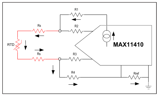
With a 2-wire RTD connection, one analog port acts as the current source output. The resistors in red represent the 2-wire RTD model. As illustrated by the arrows in Figure 2, current flows through the protection resistor (R1), the RTD wire resistance (RS), the actual RTD resistance (RTD), followed by another RS (R4), and finally through RREF. Voltage drop across RREF serves as the MAX11410 reference input. Because the MAX11410 ADC input is high impedance, the current flowing into R2 and R3 can be considered negligible. Therefore, the measured voltage of the ADC is:
VIN = I × (RS + RTD + RS)
The reference voltage of ADC in this case is:
VREF = I × RREF
Using the two equations above, the ratio of VIN to VREF can be expressed as:
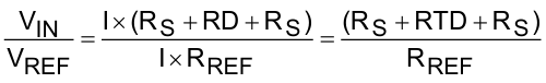
Alternatively,
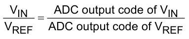
Therefore,
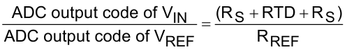
Note how the expression is independent of the current source in the expressions above.
The ADC output code for VREF is 224 for unipolar conversion. Because RREF is selected by the designer, and the ADC output of VIN would be known by reading the ADC output, the expression above can be used to calculate the (RS + RTD + RS) term, which is the RTD resistance for a 2-wire connection. The corresponding temperature value can then be calculated using a formula or lookup table.
It is important to observe that any deviation of the value of RREF from the chosen value directly affects the accuracy of the RTD resistance calculation. Therefore, a low-drift resistor with 0.1% or better is recommended. In addition, note that the RTD value calculated also includes the wire resistance. As such, a 2-wire connection is only used in short-distance temperature measurement or in cases where high accuracy is not required, so that the wire resistance can be neglected.
A 4-wire connection, which uses a Kelvin connection, is ideal for long-distance applications or those that require high accuracy. Each RTD element has two nodes, and in a 4-wire connection, two wires are connected to each RTD node. One wire from each node is connected to the ADC input. Because an ADC input has high impedance, current passes through the other wire. As such, the impact of the wire resistance is removed, allowing a 4-wire connection to achieve highly accurate measurement.
A 3-wire connection is an option that achieves highly accurate measurement with lower cost. While this type of connection removes the wire resistance in the RTD calculation, it also has one less wire compared to 4-wire connections. Therefore, 3-wire connections are the most commonly used connections in industrial applications for long-distance measurement. A 3-wire-connection measurement circuit is shown in Figure 3.
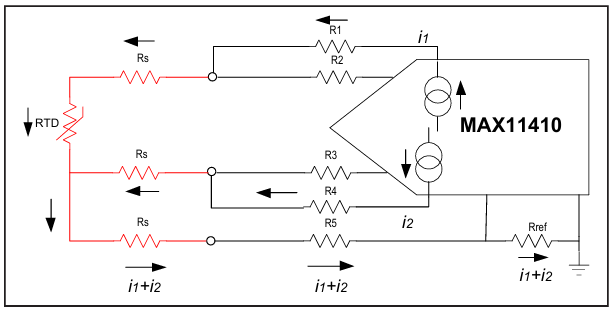
For 3-wire RTD connections, two analog ports act as current source outputs. The two current sources I1 and I2 are matched current sources, thus I1 = I2. RS is the RTD wire resistance. The resistors in red represent the 3-wire RTD resistor model. The voltage across RREF serves as the ADC reference.
The current source I1 flows through the external protection resistors R1, RS, RTD, RS, R5, and RREF. The current source I2 flows through the external protection resistors R4, RS, a second RS, R5, and RREF. Because the ADC has high input impedance, there is no current through R2 and R3, and thus, no voltage drop across the resistors. Consequently, the voltage across the two nodes where R1, R2, and RS meet and where R3, R4, RS meet can be directly measured at the ADC with no voltage loss.
The R2 input voltage is as follows:
UR2 = RS × I1 + RTD × I1 + (RS + R5 + RREF) × (I1 + I2)
The R3 input voltage is as follows:
UR3 = RS × I2 + (RS + R5 + RREF) × (I1 + I2).
The ADC input voltage is the differential voltage between UR2 and UR3, where:
UR2 - UR3 = RS × I1 + RTD × I1 + (RS + R5 + RREF) × (I1 + I2) – RS × I2 - (RS + R5 + RREF) × (I1 + I2)
Because the two current sources are matched, I1 = I2. The equation can thus be simplified as follows:
UR2 - UR3 = RTD × I1.
Note that the wire resistance is completely removed in the expression above.
Referring to the flow of current in Figure 3, the ADC reference voltage is as follows:
VREF = RREF × (I1 + I2) = 2 × I1 × RREF
Using the expressions for UR2 – UR3 and VREF, and letting:
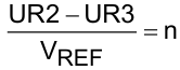
where n ≤ 0.5 if the selected RREF is the same or larger than the maximum RTD value,
RTD = n × 2 × RREF
Because the value of RREF is already known and n is the ratio of the ADC input voltage code of (UR2 - UR3) and the full-scale voltage (VREF), the RTD resistor value can be calculated. The temperature for the corresponding RTD value can then be calculated using a formula or look up table. It is important to note that two current sources flow through RREF while only one flows through RTD, and the expression for RTD is derived under the assumption that the two current sources are matched. As such, the matching of the current sources is much more important than the absolute accuracy of the current source.
With the effect of wire resistance removed, a 3-wire connection can provide highly accurate RTD measurement.
Thermocouple Measurement
Thermocouples are also commonly used in many temperature measurement applications, Thermocouples offer a cost-effective solution for measuring a much wider range of temperatures than RTDs, and they feature ruggedness and a fast response time.
A thermocouple (see Figure 4) is constructed with two wires made from dissimilar metals. One wire is predesignated as the positive side and the other as the negative side. There are many thermocouple types such as K-type, T-type, and so on. Each thermocouple type offers a unique thermoelectric characteristic over its specified temperature range.
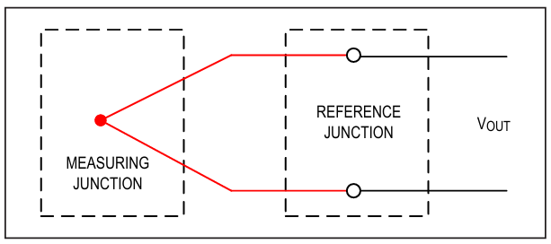
If the measuring (hot) junction temperature is different from reference (cold) junction temperature, a potential difference (VOUT) forms across the two junctions. This voltage is a function of the difference between hot and cold junction temperatures.
If the cold junction temperature is 0°C, the voltage measured is a direct translation of the actual hot junction temperature. Otherwise, we would need to know the cold junction temperature in addition to VOUT to calculate the hot junction temperature. This is known as cold-junction compensation. Cold junction temperature can be measured using different kinds of temperature sensors. For accurate cold junction temperature measurement, RTD is the best choice as it provides high accuracy and fast response time.
Figure 5 illustrates the configuration used in this reference design for thermocouple temperature measurement where RTD is the cold junction temperature compensation.
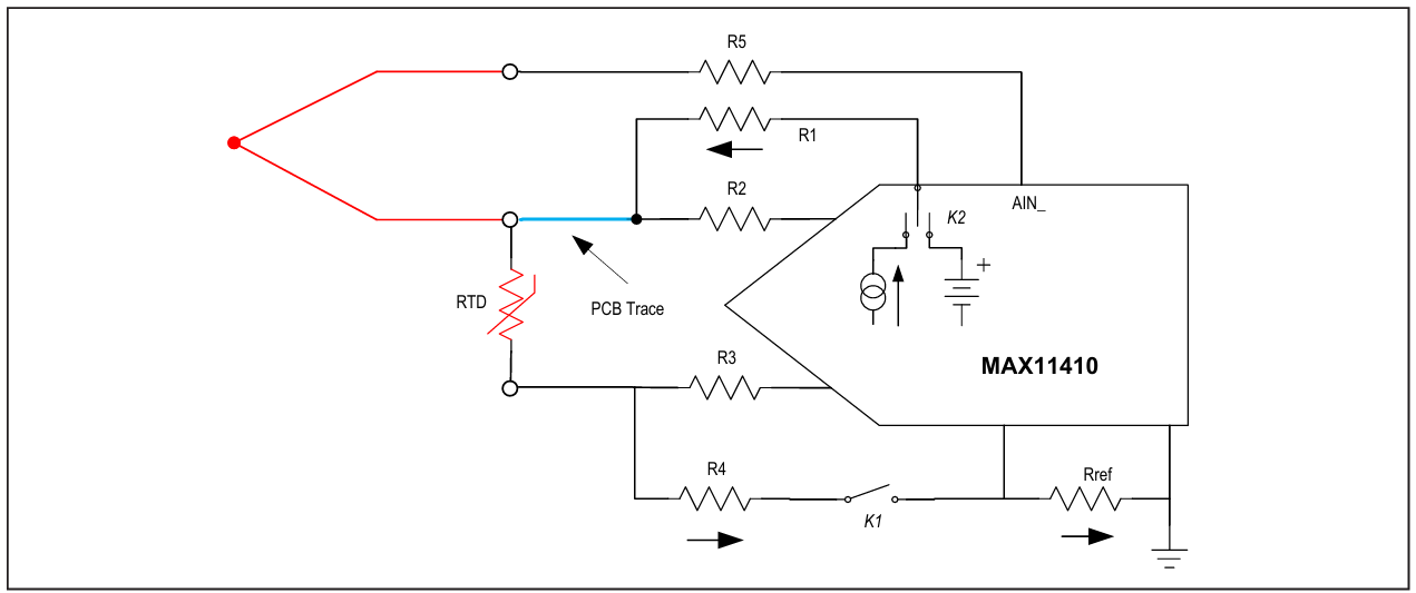
In Figure 5, RTD is used for cold junction temperature measurement. RTD is configured in a 2-wire connection and is placed as close as possible to the cold junction to measure its temperature accurately. The ADC measures the thermocouple output voltage using one ADC input channel shared between the thermocouple, RTD, and a second ADC input channel (AIN_). When performing thermocouple voltage measurement, K2 is switched to a bias voltage source to provide a bias voltage to the thermocouple. This provides a suitable common-mode input voltage for ADC measurement. Meanwhile, K1 is open to help reduce the error introduced by the PCB trace. This may be necessary as the output voltage of the thermocouple is very small and any error can affect the accuracy. Because the output of a thermocouple is voltage, an external precision voltage reference (not shown in Figure 5) is used as the ADC reference. The differential ADC input voltage can be amplified by an internal PGA before being converted by the ADC.
The cold junction temperature measured by the RTD is converted to a corresponding thermocouple output voltage before being added to the thermocouple output voltage. The sum of the two voltages is the voltage generated by hot junction temperature with reference to 0°C. The corresponding temperature can be obtained by using a formula or lookup table.
Design Procedure for MAXREFDES1154
This section describes the components of the MAXREFDES1154. Figure 6 is a block diagram of the system.
Step 1: Analog Front End Design
The MAXREFDES1154 is designed for 4-channel input where each channel can be configured as a 2-wire or 3-wire RTD, or thermocouple with 2-wire RTD as cold junction compensation. A multiplexer is used to configure the analog front end (AFE) for different input configurations and to switch between four different channels.
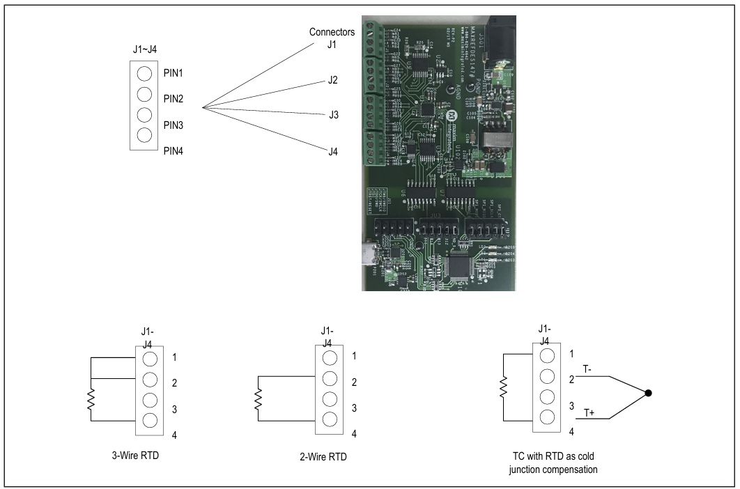
For simplification, Figure 7 shows an AFE for a single channel for all the supported input configurations and illustrates how the RTD and TC need to be connected. For example, for TC with RTD as cold compensation, one end of the TC needs to be connected to node 1, the other end of the TC needs to be connected to node 2, one end of the 2-wire RTD needs to be connected to node 1, and the other end of the RTD needs to be connected to node 3.
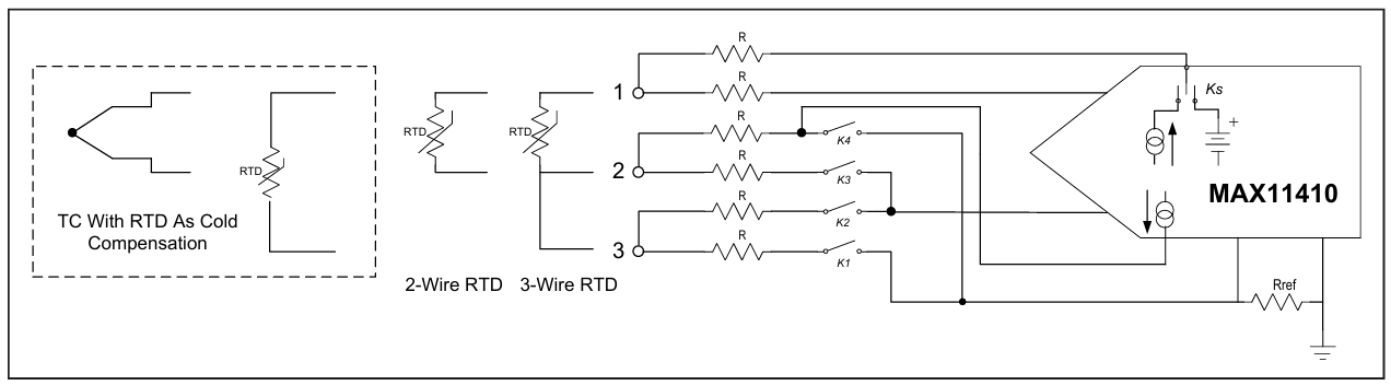
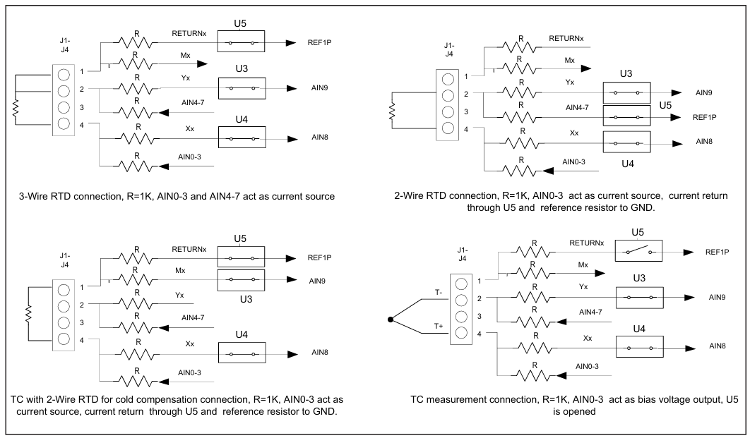
For 3-wire RTD measurement, KS is switched to a current source output, and the second matching current source also outputs current with the K4 switch left open. This forces the current flow through the RTD wire. K1 is closed for current return, resulting in both current sources flowing through RREF. K3 is closed to connect node 2 to the ADC input and K2 is left open. The ADC measures the voltage between node 1 and node 2 using RREF as the ADC reference.
For 2-wire RTD measurement, RTD is connected between node 1 and node 2. Only one current source is used to drive RTD. KS is switched to a current source output. The other current source is configured as an ADC input so that it exhibits high input impedance. K4 is closed for current return, and K3 is closed to connect node 2 to the ADC input. K1 and K2 are left open. The ADC measures the voltage between node 1 and node 2 using RREF as the ADC reference.
For thermocouple measurement using RTD for cold junction temperature compensation, RTD is connected between node 1 and node 3, and a thermocouple is connected between node 1 and node 2. Two-step measurement is required to determine temperature. The cold junction temperature is measured with 2-wire RTD, followed by the thermocouple output voltage.
For cold junction temperature 2-wire RTD measurement, only one current source is used to drive the RTD. KS is switched to a current source output, K1 is closed for current return, and K2 is closed for RTD measurement. K3 and K4 are left open. The ADC measures the voltage between node 1 and node 3 with RREF as the ADC reference.
For thermocouple voltage measurement, the thermocouple is connected between node 1 and node 2. KS is switched to bias-voltage output to supply-bias voltage to the thermocouple output. K1, K2 and K4 are kept open to reduce leakage current. K3 is closed to connect node 2 to the ADC input. The ADC measures the voltage between node 1 and node 2 with the external voltage reference as the ADC reference.
To implement four channels, two matched current sources internal to MAX11410 are directly connected to the four different channels J1 to J4 through AIN0 to AIN7 of MAX11410 in the schematic. The MAX11410 allows each current source to be connected to at most one of the analog inputs, providing the capability to select which of the four channels each current source is routed. AIN8 and AIN9 of MAX11410 serve as the ADC input for measurement for all the input configurations. A 4:1 multiplexer, MAX4704 (U4), is used to switch between the four different channels J1 to J4 to go to the positive differential input AIN8. The switching functionality of K1 and K4 is implemented by MAX4617, an 8:1 multiplexer (U5). K1 and K4 each needs four analog switches for four different channels. Similarly, the switching functionality for K2 and K3 is implemented by another MAX4617 (U3). Instead of having four separate 4:1 multiplexers for each of K1 to K4, two 8:1 multiplexers are used. Sharing multiplexers is possible because neither K1 or K4 is turned on at the same time, as is the case for K2 and K3.
Figure 8 shows how the sensor should be connected for the three different configurations on the PCB. For example, for 2-wire RTD, one end should be connected to PIN2 of J1 to J4 and the other end should be connected to PIN4 of J1 to J4. Please note that node 1, node 2, and node 3 in Figure 7 correspond to PIN4, PIN2, PIN1 on J1 to J4 on the schematic respectively. In other words, Figure 7 is inverted from the connection on the schematic.
With the input RTD/TC properly connected, Figure 9 illustrates how the current/bias voltage source and the switch are configured on the schematic for the supported input configurations. For example, in 3-wire RTD, one of the inputs from AIN0 to AIN3 and one of the inputs from AIN4 to AIN7 serve as the two current sources required. By closing the switch in U5 for ground return, RETURNx is connected to REF1P which is then connected to the two reference resistors R25 and R26. By closing the switch in U3, Yx is connected to AIN9, which is the negative differential analog input. Xx is connected to AIN8, the positive differential analog input. As a result of these connections, the two current sources flow from one of AIN0 to AIN3 and one of AIN4 to AIN7 and return through RETURNx. Note that RETURNx and Yx correspond to K1 and K3 in Figure 7, respectively. K2 and K4 are not shown as they are left open.
With the switches properly designed, the next design decision is related to the reference selection and the internal PGA gain selection of MAX11410 to maximize the use of the ADC output range while satisfying the ADC parameters. The maximum compliance voltage of the MAX11410 output current source is AVDD – 0.7V when IDAC ≤ 250µA. In this system, AVDD is 3.3V, and thus, the maximum voltage is 2.6V.
For 3-wire PT100 applications, select a current source of 200µA to ensure that the output voltage of the current source is less than 2.6V. The compliance voltage of the KS output current source is (R + RRTD) × 200µA + (R + RREF) × 200µA × 2, where R is a 1kΩ protection resistor. For 3-wire PT100 and PT1000 applications, select a minimum of 4kΩ to meet the RREF requirements. The resistor value of RRTD is approximately 391Ω at 850°C for PT100 applications. If the value of RRTD is rounded up to 400Ω, the KS output current voltage is (1k + 0.4k) × 200µA + (4k + 1k) × 200µA × 2 = 2.28V. The voltage headroom is 0.32V, which shows that an RTD wire resistor up to 500Ω can be supported. PGA gain is set to 16 to maximize utilization of the ADC output range.
For 2-wire PT100 applications, select a current source of 300µA. Only one current source is used in a 2-wire connection, so the current source output voltage is (1k + 0.4k) × 300µA + (4k + 1k) × 300µA = 1.92V. Because RREF is 4kΩ, and the RTD resistor value is approximately 391Ω at 850°C, PGA gain is set to 8 to maximize the utilization of the ADC output range.
For thermocouple measurement, the low noise, high-precision voltage reference MAX6071AAUT12 is used as the reference. The MAX6071AAUT12 is a voltage reference with ±0.04% initial accuracy and 1.5ppm/°C (typ) temperature drift. High accuracy, low drift, and low noise make it suitable for high accuracy measurement. Because different types of thermocouples have different output voltage ranges, PGA gain is set to 8 to support all types of thermocouples while maximizing the utilization of the ADC output range. The maximum measured voltage is approximately 8 × 78mV = 0.624V.
The current source/bias voltage and PGA gain settings for different input configurations can be found in Table 2.
| Input Type | Current/Bias Voltage | PGA | Note |
| Thermocouple | Bias Voltage | 8 | Current source disabled |
| PT100 for Thermocouple | 300µA | 8 | One current source |
| PT1000 for Thermocouple | 200µA | 1 | One current source |
| 3-Wire PT100 | 200µA | 16 | Two current sources |
| 2-Wire PT100 | 300µA | 8 | One current source |
| 3-Wire PT1000 | 100µA | 2 | Two current sources |
| 3-Wire PT1000 | 200µA | 1 | One current source |
Step 2: Sensor Open Detection
For system reliability and safety, the system detects sensor fault conditions such as when a sensor is improperly connected. The integrated burnout current source in the MAX11410 is connected to the positive analog input, and the current sink is connected to the negative analog input. If there is an open circuit in the sensor input path, the burnout current source and sink pulls the positive input towards AVDD and the negative input towards AGND, respectively. This results in a full-scale reading and indicates that there is an open circuit at the sensor input. In addition to from open fault detection, this feature can also help detect if a 2-wire RTD or 3-wire RTD connection is present.
Step 3: Power Supply Design
The measurement system is powered by a field 24V power supply. Field power supplies are very noisy and are highly susceptible to interference in harsh industrial environments, which can result in poor analog measurement accuracy. Therefore, an iso-buck MAX17681 is used to generate an isolated 5.5V supply to isolate the field power supply from the system power supply. Because the analog section requires a very stable power supply to ensure high accuracy, a low-cost LDO (MAX16910) is used to generate a +3.3V power supply to power the analog multiplexer, reference, and ADC. The LDO is supplied by the isolated 5.5V power supply.
Step 4: Protection Design
To prevent a high-voltage transient pulse at the power supply input from damaging the device, a voltage regulator made with a Zener diode and the MMBT3904 by ON Semiconductor® is added. This voltage regulator can handle up to a 65V transient pulse.
The MAX4617 can handle a ±75mA continuous current into any of the terminal pins, and the MAX4704 can handle a ±20mA continuous current into any of the terminal pins. At each input terminal pin, there is a 1k protection resistor in series to limit the current into the analog input terminal. With this protection, up to ±30V input voltage can be applied across any two terminals without damaging the internal circuitry.
Step 5: Digital Isolation Design
A microcontroller configures the ADC and reads the ADC conversion results through the SPI interface. The MAX14931 is used to isolate the SPI communication signals between the MCU and the analog front end. The MAX14930 is used to isolate the multiplexer control signals. Only one MAX14930B and one MAX14931B are required to achieve the digital isolation between the microcontroller and the analog front end and ADC.
The MAX14930B/MAX14931B is a 4-channel, 2.75kVRMS digital isolator that supports up to a 25Mbps data rate. Low propagation delay makes the device suitable for supporting high speed SPI communication isolation.
Microcontroller Design
The MAXREFDES1154 uses the on-board microcontroller to evaluate the performance of the RTD/TC temperature measurement. The on-board LDO (MAX16910) generates the 3.3V power supply to power the microcontroller. The MAX16910 used for the microcontroller is supplied through USB power. The MAX6730A watchdog monitor device is used to monitor the microcontroller to make sure that it works properly and is an open-drain output with a long initial watchdog timeout period (35s minimum) and a short timeout period (1.12s) after the first valid WDI transition. The long initial watchdog timeout provides enough time to initialize the system after power up. The MAX6730A is populated on the board but is not implemented in the firmware.
The MAXREFDES1154 also supports communication using an external microcontroller. Remove the jumpers on JU2 and JU3 and connect external SPI and GPIO signals to JU2 and JU3. This allows the customer to evaluate the analog front end with different microcontrollers or custom firmware easily.
The MAXREFDES1154 uses the on-board STM32F1 microcontroller by STMicroelectronics® to control the analog multiplexers and communicate with the ADC. The user reads the sampled data through a terminal program, allowing analysis on any third-party software. The user can also perform system calibrations through a terminal program. The simple process flow is shown in Figure 10. The firmware is developed in C using the IAR tool.
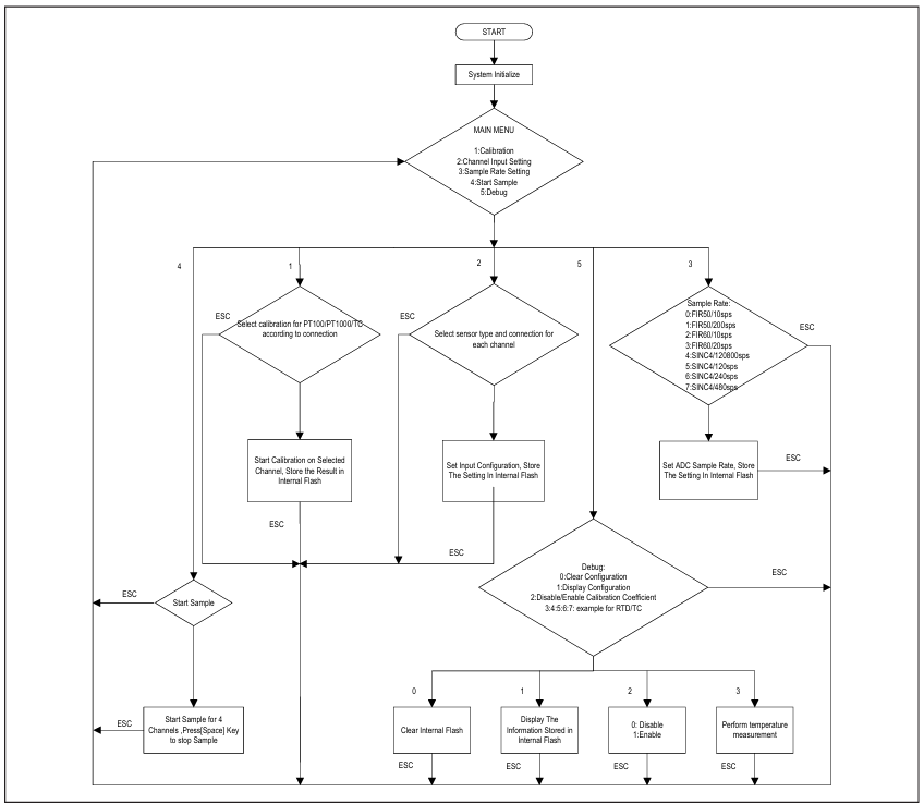
The firmware can perform channel setting, calibration, sampling and accept debug commands. Communication with a PC is achieved through a standard terminal program using a virtual COM port.
Complete source code is provided to speed up customer development. Code documentation can be found in the corresponding firmware platform files.
関連資料
-
MAXREFDES1154 Design Files2021/02/15ZIP11M
-
MAXREFDES1154: Configurable 4-Channel RTD/TC Measurement System Using the MAX114102021/02/15PDF799 K
サポートおよびトレーニング
技術的なご質問についての回答は、ナレッジベースを検索してください。また、アナログ・デバイセズのアプリケーション・エンジニアの専任チームが、技術的なご質問にお答えいたします。