Simple Circuit Boosts a 3V Input and Improves Efficiency
要約
In this design note a synchronous buck converter, the MAX1967, and a charge pump improve low-input voltage efficiency. The circuit boosts the 3V input to a 5V output. with a 3% rise in efficiency for a 0.35W power savings.
The MAX1967 is a voltage mode PWM synchronous buck controller that is ideal for a variety of cost-sensitive applications. Fixed 100kHz switching frequency allows cheap aluminum electrolytic capacitors and powdered-iron core magnetics to be used for minimum-cost designs. The MAX1967 has an input range of 2.7V to 28V. A drawback with low-voltage inputs like 3.3V is that efficiency is penalized due to low gate drive for the external MOSFETs, which exhibit higher on-resistance. This application note shows how to improve low input voltage efficiency by boosting the gate drive supply voltage with a simple diode-capacitor charge pump circuit.
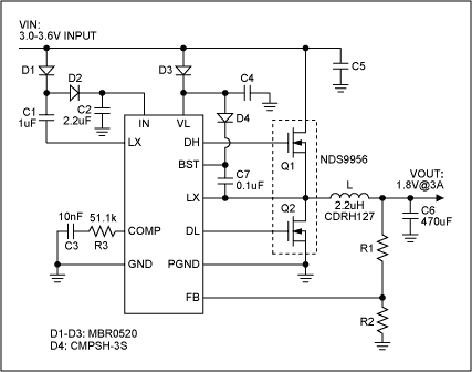
In Figure 1, a discrete charge pump composed of D1, D2, C1 and C2 boosts the input voltage. The voltage at the IN pin is 2 times the input voltage, Vin. This is fed to the MAX1967's internal linear regulator input to generate a 5V output, VL. Thus, the 5V gate drive is provided to the external MOSFET, even with a 3V input. D3 is used to start up the IC during the soft start. Once the IC and the charge pump circuit start to operate, VL provides 5V output, which reverses bias diode D3.

Figure 1. Synchronous buck converter with charge pump.
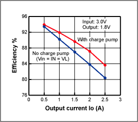
Figure 2 shows conversion efficiency with 3.0V input and 1.8V output. It is shown that the measured efficiency with the charge pump is 3% higher than that of conventional connection (IN and VL tie to input) at a 2.5A load. This results in 0.35W power savings and reduces heat dissipation.

Figure 2. Measured efficiency vs output current.