AN-2546: Automotive SENT Interface-Based Thermocouple Temperature Sensor with Cold Junction Compensation Using the ADuC7060/ADuC7061 Precision Analog Microcontroller
Circuit Function and Benefits
The circuit shown in Figure 1 uses the ADuC7060 or the ADuC7061 precision analog microcontroller in an accurate thermocouple temperature monitoring application. The ADuC7060/ADuC7061 integrate dual 24-bit sigma-delta (Σ-Δ) analog-to-digital converters (ADCs), dual programmable current sources, a 14-bit digital-to-analog converter (DAC), and a 1.2 V internal reference, as well as an ARM7 core, 32 kB flash, 4 kB SRAM, and various digital peripherals such as UART, timers, serial peripheral interface (SPI), and I2C interfaces.

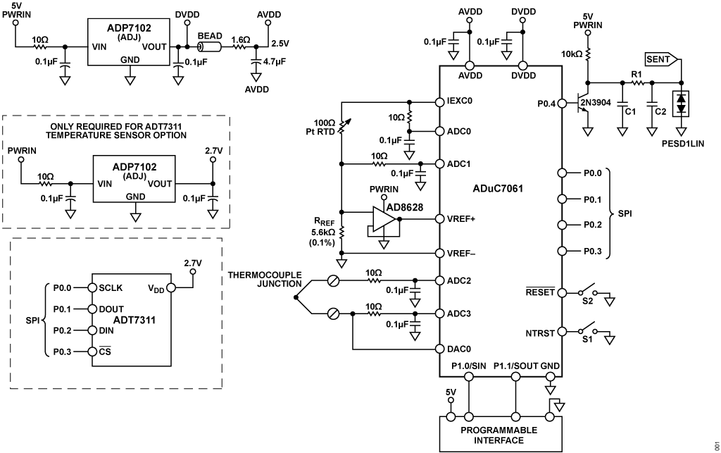
Figure 1. ADuC7060/ADuC7061 as a Temperature Monitor Controller with a Thermocouple Interface (Simplified Schematic, All Connections Not Shown).
In the source code, an ADC sampling rate of 4 Hz was chosen. When the ADC input programmable gain amplifier (PGA) is configured for a gain of 32, the noise-free code resolution of the ADuC7060/ADuC7061 is greater than 18 bits.
The single edge nibble transmission (SENT) interface to the host is implemented by using a timer to control a digital output pin. This digital output pin is then level shifted externally to 5 V using an external NPN transistor. An EMC filter is provided on the SENT output circuit as recommended in Section 6.3.1 of the SENT protocol (SAE J2716 Standard). The data is measured as falling edge to falling edge, and the duration of each pulse is related to the number of system clock ticks. The system clock rate is determined by measuring the SYNC pulse. The SYNC pulse is transmitted at the start of every packet. More details are provided in the SENT Interface section.
Circuit Description
The following features of the ADuC7060/ADuC7061 are used in this application:
- A primary, 24-bit ∑-Δ ADC with a PGA. The PGA is set for a gain of 32 in the software for this application. The primary ADC was switched continuously between sampling the thermocouple and the RTD voltages.
- If an RTD is used for measuring the cold junction temperature, programmable excitation current sources force a controlled current through the RTD. The dual current sources are configurable in 200 µA steps from 0 µA to 2 mA. For this example, a 200 µA setting was used to minimize the error introduced by the RTD self-heating.
- If the ADT7311 is used for measuring the cold junction temperature, the SPI interface is used in master mode to connect the ADT7311 slave device.
- An internal 1.2 V reference for the ADC in the ADuC7060/ADuC7061. For measuring the thermocouple voltage, the internal voltage reference was used due to its precision.
- An external voltage reference for the ADC in the ADuC7060/ADuC7061. For measuring the RTD resistance, a ratiometric setup was used where an external reference resistor (RREF) was connected across the external VREF+ and Vref− pins.
- The AD8628 single supply op amp was used to buffer the high impedance reference voltage across RREF to the ADC.
- The OP193 is another option instead of the AD8628.
- A DAC that was used to set the thermocouple common-mode voltage to 850 mV above ground.
- An ARM7TDMI® core. The powerful 16-/32-bit ARM7 core with integrated 32 kB flash and SRAM memory runs the user code that configures and controls the ADC, processes the ADC conversions from the RTD, and controls the communications over the SPI interface.
- Timer1 and a digital output pin are used to generate the SENT output signal.
- An optional PESDLIN protection diode for suppression of ESD, electrical fast transients (EFT), and surge transients up to 23 kV.
- An EMC filter on the SENT output as recommended in Section 6.3.1 of the SAE J2716 standard (SENT Protocol).
- Two external switches are used to force the part into its flash boot mode. By holding S1 low and toggling S2, the ADuC7060/ADuC7061 enter boot mode instead of normal user mode. In boot mode, the internal flash can be reprogrammed through the UART interface.
Both the thermocouple and the RTD generate very small signals; therefore, a PGA is required to amplify those signals. As the auxiliary ADC on the ADuC7060/ADuC7061 does not have a PGA, both were connected to the primary ADC, and switching between the two was done in software.
The thermocouple used in this application is a Type T (copper-constantan), which has a temperature range of −200°C to +350°C. Its sensitivity is approximately 40 µV/°C; therefore, in bipolar mode, the ADC, with a PGA gain of 32, can cover the entire temperature range of the thermocouple.
The RTD was used for cold junction compensation. In this circuit, a platinum, 100 Ω RTD, Enercorp PCS 1.1503.1 was used. It is available in a 0805 surface-mount package. This RTD has a temperature variation of 0.385 Ω/°C.
Note that the reference resistor, RREF, should be a precision 5.6 kΩ (±0.1%).
SENT Interface
The SENT interface is a single pin, unidirectional (sensor to host), time modulated signal used mainly in automotive systems for interfacing distributed sensors to host CPUs.
The main requirements for SENT include the following:
- It must have a 0 V to 5 V signal swing with EMC filtering.
- The clock used for the SENT signal must be accurate to ±20%.
- The SENT output circuit must be robust enough to tolerate short circuit to ground and short circuit to supply voltages.
The associated source code uses the P0.4 digital pin of the ADuC7061 as the SENT output pin. The packet format used is the single sensor packet format as detailed in A.4 section of the SAE J2716 standard (SENT Protocol) document. The source code, particularly the SENT.h and Sent.c files can be modified to support other packet formats. The overall temperature result is returned in /°C format in Data Nibble 1 to Data Nibble 3. In summary, the returned output packet is:
- 56 clock ticks for sync pulse
- Status pulse (7 ticks to 15 ticks)
- Data Nibble 1 (Bit 11 to Bit 8 of the temperature result)
- Data Nibble 2 (Bit 7 to Bit 4 of the temperature result)
- Data Nibble 3 (Bit 3 to Bit 0 of the temperature result)
- Data Nibble 4 (Bit 7 to Bit 4 of the counter)
- Data Nibble 5 (Bit 3 to Bit 0 of the counter)
- Data Nibble 6 (inverse of Nibble 1)
An example packet is shown in Figure 2.

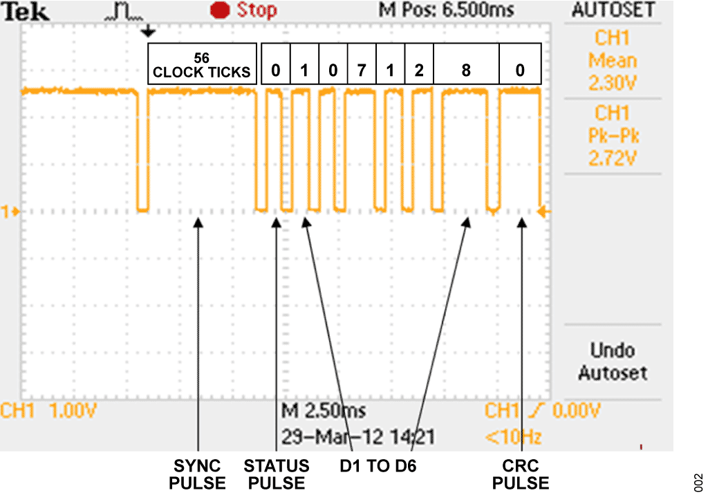
Figure 2. Example SENT Packet Measured at the P0.4 Pin.
The circuit must be constructed on a multilayer printed circuit board (PCB) with a large area ground plane. Proper layout, grounding, and decoupling techniques must be used to achieve optimum performance (see Tutorial MT-031, Grounding Data Converters and Solving the Mystery of "AGND" and "DGND," Tutorial MT-101, Decoupling Techniques, and the ADuC7060/ ADuC7061 evaluation board layouts).
Code Description
Timer1 is used to control the SENT output pin, P0.4. When a temperature result is been calculated from the ADC results for the thermocouple and the cold junction temperature, the SENT packet structure, SENT_PACKET, is updated, and Timer1 started. The fields of the structure are clocked out on the P0.4 pin, as shown in Figure 2. The first stage of the packet is the sync sequence. The host determines the clock period from this pulse, and it determines the subsequent nibble values from this.
To get a temperature reading, measure the temperature of the thermocouple and the RTD. The RTD temperature is converted to its equivalent thermocouple voltage via a lookup table. These two voltages are added together to give the absolute value of the voltage at the thermocouple.
First, the voltage between the two wires of the thermocouple (V1) is measured. Then, the RTD voltage is measured and converted to a temperature via a lookup table. This temperature is then converted to its equivalent thermocouple voltage (V2). V1 and V2 are then added to give the overall thermocouple voltage, and this value is then converted to the final temperature measurement.
A piecewise linearization scheme is used to calculate the final temperature value. The respective temperatures for a fixed number of voltages are stored in an array, and values in between are calculated using a linear interpolation between the adjacent points. Figure 3 gives the algorithm error using the ideal thermocouple voltages. Figure 4 shows the error obtained when using the ADC0 pin on the ADuC7060/ADuC7061 to measure the 52 thermocouple voltages over the full thermocouple operating range. The overall worst-case error is <1°C.

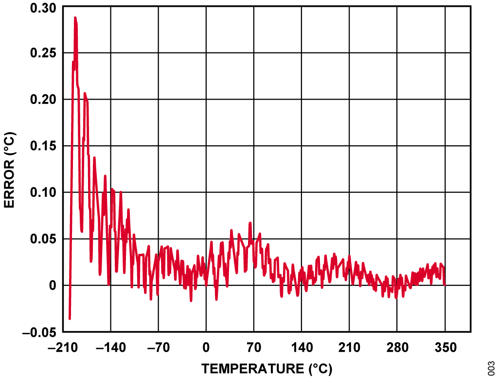
Figure 3. Error When Using Piecewise Linear Approximation Using 52 Calibration Points and Ideal Measurements.

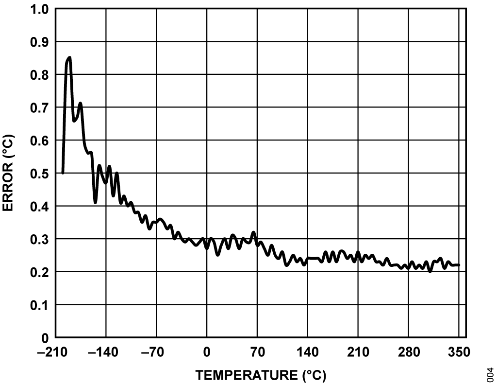
Figure 4. Error When Using Piecewise Linear Approximation Using 52 Calibration Points Measured by the ADC0 Pin of the ADuC7060/ADuC7061
The RTD temperature is calculated using lookup tables and is implemented for the RTD the same way as for the thermocouple. Note that the RTD has a different polynomial describing its temperatures as a function of resistance.
The source code in the design support package was generated using KEIL µVision V3.90.
For details on linearization and maximizing the performance of the RTD, refer to Application Note AN-0970, RTD Interfacing and Linearization Using an ADuC706x Microcontroller.
Circuit Evaluation and Tests
SENT Interface Tests
The SENT interface output was evaluated using a digital oscilloscope and a logic analyzer. The SENT interface was only tested with a SENT clock period of 100 µs, which is the maximum allowed by the SENT standard. The limiting factors in this implementation include the following:
- Variation in FIQ interrupt latency for the timer. The interrupt latency of an ARM7 can be up to 45 CPU clocks. With a 10.24 MHz CPU clock, this is up to 4.4 µs. The minimum is 5× CPU clocks (0.5 µs). The worst-case latency occurs when the ARM7 core is executing a LDMIA or STMIA (load or store multiple values to/from memory). Select the Split Load and Store Multiple compiler option to minimize this, and see Figure 5 to see how to do this.

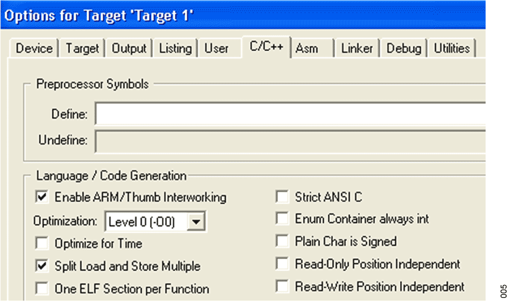
Figure 5. Selecting Split Load and Store Multiple Option.
- The 10.24 MHz oscillator on the ADuC7060/ADuC7061 has a worst-case accuracy of ±3% over the −40°C to +125°C operating temperature range.

Despite these limitations, this implementation is well within the required ±20% timing accuracy of the SENT specification when a SENT clock period of 100 µs is selected.
An EMC filter has been catered for on the SENT output in Figure 1. Chose values for this filter (R1, C1, C2) to meet the targeted transmitter output waveform, as shown in Figure 6, to reduce EMC emissions due to the SENT output.

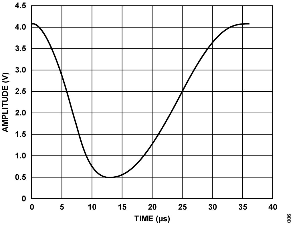
Figure 6. Example SENT Shaped Waveform Transmitter Output.
Only limited testing of this filter has been done; therefore, the resistor and capacitor values for the output filter were omitted, as is shown in Figure 1 (R1, C1, and C2).
To further test and evaluate the circuit, the thermocouple measurements and the RTD measurements were evaluated separately.
Thermocouple Measurement Test
Two methods were used to evaluate the performance of the circuit. Initially, the circuit was tested with the thermocouple attached to the board and used to measure the temperature of an ice bucket, and then the temperature of boiling water.
A Wavetek 4808 multifunction calibrator was used to fully evaluate the error, as shown in Figure 3 and Figure 4. In this mode, the thermocouple was replaced with the calibrator as the voltage source, as shown in Figure 7. To evaluate the entire range of a Type T thermocouple, the calibrator was used to set the equivalent thermocouple voltage at 52 points between −200°C to +350°C for the negative and positive ranges of the Type T thermocouple (see the ITS-90 Table for Type T thermocouple).

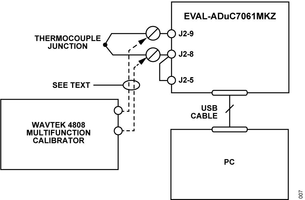
Figure 7. Test Setup Used to Calibrate and Test the Circuit Over Full Thermocouple Output Voltage Range.
To evaluate the accuracy of the lookup algorithm, 551 voltage readings, equivalent to temperatures in the range of −200°C to +350°C spaced at +1°C, were passed onto the temperature calculation functions. Errors were calculated for the linear method and the piecewise linear approximation method as can be seen in Figure 3 and Figure 7.
RTD Measurement Test
To evaluate the RTD circuit and linearization source code, the RTD on the board was replaced with an accurate, adjustable resistance source. The instrument used was the 1433-Z decade resistor. RTD values from 90 Ω to 140 Ω, which represent an RTD temperature range of −25°C to +114°C, was the range of the RTD values tested.
The error results for the RTD tests are shown in Figure 8, and the setup circuit is shown in Figure 9.


Figure 8. Error in °C of the RTD Measurement Using Piecewise Linearization Code and ADC0 Measurements.

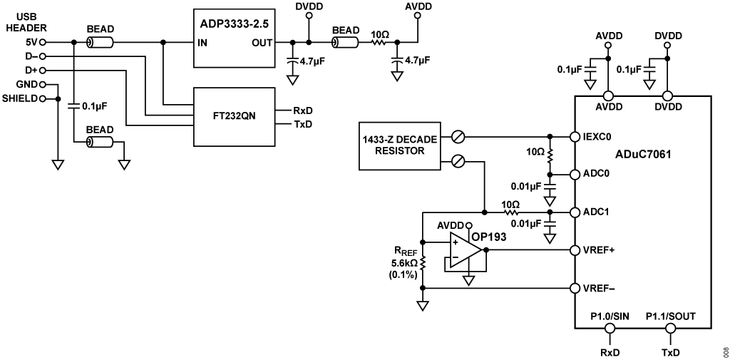
Figure 9. Test Setup Used to Calibrate and Test the RTD Output Voltage Range from −25°C to +114°C.