AD4085
新規設計に推奨16-Bit, 10 MSPS, Low Noise, Low Power SAR ADC
Low Noise, Low Power, Fast Precision SAR ADC
- 製品モデル
- 3
- 1Ku当たりの価格
- 最低価格:$23.61
製品情報
- 16-bit resolution, no missing codes
- Throughput: 10MSPS, 131.25ns conversion latency
- Noise spectral density: 20.85nV/√Hz,−160.1dBFS/Hz
- Low 1/f, low frequency noise (0.1Hz to 10Hz): 206.4nV rms
- Low power: 57.8mW typical at 10MSPS
- INL: ±5ppm (typ), ±10ppm (max)
- Dynamic range: 93.2dBFS
- SNR/THD
- 92.9dB (typ)/−114dB (typ) at fIN = 1kHz
- 92.5dB (typ)/−102.9dB (typ) at fIN = 1MHz
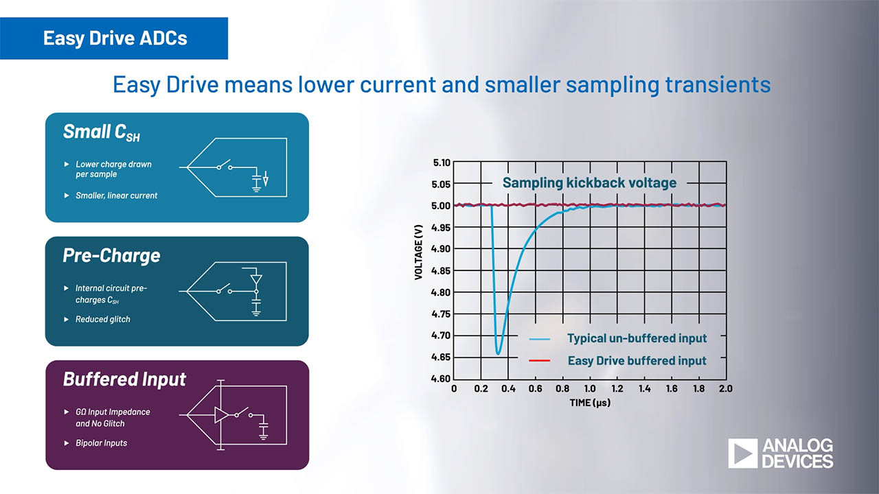
- Easy Drive
- 6V p-p differential input range
- Continuous signal acquisition
- Linearized, 5μA/MSPS input current
- Integrated, low-drift reference buffer and decoupling
- Integrated VCM generation
- Digital features and data interface
- Conversion result FIFO, 16K sample depth
- Digital averaging filter with up to 210 decimation
- SPI configuration
- Configurable data interface
- Single lane, DDR, serial LVDS, 160Mbps per lane
- Dual lane, DDR, serial LVDS, 80Mbps per lane
- Single/quad lane SPI data interface
- Package
- 49-ball, 5mm × 5mm CSP_BGA, 0.65mm pitch
- Integrated supply decoupling capacitors
- Operating temperature range: −40°C to +85°C
The AD4085 is a high speed, low noise, low distortion, 16-bit, Easy Drive, successive approximation register (SAR) analog-to-digital converter (ADC). Maintaining high performance (signal-to-noise and distortion (SINAD) ratio > 92dBFS) at signal frequencies in excess of 1MHz enables the AD4085 to service a wide variety of precision, wide bandwidth data acquisition applications. Simplification of the input anti-alias filter design can be accomplished by applying oversampling along with the integrated digital filtering and decimation to reduce noise and lower the output data rate for applications that do not require the lowest latency of the AD4085.
The AD4085 Easy Drive features reduce both signal chain complexity and power consumption while enabling greater channel density and flexibility in companion component selection. The product input structure was designed to minimize any input dependent signal currents, therefore reducing any converter induced settling artifacts. The continuous acquisition architecture allows settling across the entire conversion cycle, easing ADC driver settling and bandwidth requirements as compared to other high-speed data converters.
The AD4085 includes several elements that simplify data converter integration: a low drift reference buffer, low dropout (LDO) regulators to generate ADC core and digital interface supply rails, and a 16K result data first-in first out (FIFO) that can greatly reduce the load on the digital host. Additionally, critical supply and reference decoupling capacitors are integrated in the package to ensure optimum performance, simplify printed circuit board (PCB) layout, and reduce the overall solution footprint.
APPLICATIONS
- Digital imaging
- Cell analysis
- Spectroscopy
- Automated test equipment
- High speed data acquisition
- Digital control loops, hardware in the loop
- Power quality analysis
- Source measurement units
- Electron and X-ray microscopy
- Radar level measurement
- Nondestructive test
ドキュメント
データシート 1
ユーザ・ガイド 1
ビデオ 2

デバイス・ドライバ 1
ウェブキャスト 2
| 製品モデル | ピン/パッケージ図 | 資料 | CADシンボル、フットプリント、および3Dモデル |
|---|---|---|---|
| AD4085BBCZ | 49-ball CSP_BGA (5 mm x 5 mm x 1.33 mm) | ||
| AD4085BBCZ-RL | 49-ball CSP_BGA (5 mm x 5 mm x 1.33 mm) | ||
| AD4085BBCZ-RL7 | 49-ball CSP_BGA (5 mm x 5 mm x 1.33 mm) |
これは最新改訂バージョンのデータシートです。
ソフトウェア・リソース
デバイス・ドライバ 1
必要なソフトウェア/ドライバが見つかりませんか?
ハードウェア・エコシステム
| 製品モデル | 製品ライフサイクル | 詳細 |
|---|---|---|
| オペアンプ(OPアンプ) 1 | ||
| ADA4899-1 | 製造中 | オペアンプ、高速、安定したユニティ・ゲイン、超低歪み、1nV/√Hz |
| スイッチング・レギュレータ & コントローラ 3 | ||
| LT8604 | 新規設計に推奨 | 高効率42V/120mA同期降圧 |
|
LT8606 LT8606B |
静止電流が2.5μAの42V、350mA同期整流式降圧レギュレータ | |
| MAX1606 | 製造中 | 28V内蔵スイッチ、LCDバイアス電源、True Shutdown™付 |
| パワー・システム・マネージメント(PSM) & シーケンサ 1 | ||
| ADM1085 | 製造中 | アクティブ・ハイ/オープン・ドレイン・イネーブル出力の電圧シーケンサ |
| ファンアウト・バッファ 1 | ||
| AD9508 | 新規設計に推奨 | クロック・ファンアウト・バッファ、1.65GHz、出力デバイダおよび遅延調整機能付 |
| フェーズ・ロック・ループ(PLL)シンセサイザ 1 | ||
| ADF4350 | 製造中 | 広帯域シンセサイザ、VCO内蔵 |
| リニア・レギュレータ 6 | ||
| MAX38912 | 新規設計に推奨 | 11µVRMS低ノイズ、500mA LDOリニアレギュレータ、低電力モード内蔵 |
| LT3045 | 新規設計に推奨 | 20V、500mA、超低ノイズ、超高PSRRのリニア・レギュレータ |
| ADP150 | 製造中 | リニア・レギュレータ、150mA、超低ノイズ、CMOS |
| ADP7182 | 新規設計に推奨 | リニア・レギュレータ、-28 V / − 200 mA、低ノイズ |
| ADP7118 | 新規設計に推奨 | 20V、200mA、低ノイズ、CMOS LDOリニア電圧レギュレータ |
| LT3093 | 新規設計に推奨 | -20 V、200 mA、超低ノイズ、超高 PSRR、負電圧のリニア電圧レギュレータ |
| 監視回路 & リセットIC 1 | ||
| MAX16061 | 新規設計に推奨 | 精度1%、クワッド/ヘックス(6回路)/オクタル(8回路)電圧µP監視回路 |
| 差動アンプ 2 | ||
| ADA4945-1 | 新規設計に推奨 | 高速でオフセット・ドリフトが ±0.1µV/°Cの完全差動ADC用ドライバ |
| ADA4930-1 | 新規設計に推奨 | 超低ノイズ・ドライバ・アンプ、低電圧 A/D コンバータ向け |
| 電圧リファレンス 2 | ||
| LTC6655 | 製造中 | ノイズが0.25ppmの低ドリフト高精度リファレンス |
| ADR4530 | 製造中 | 3.0V電圧リファレンス、超低ノイズ、高精度 |
ツールおよびシミュレーション
IBISモデル 1
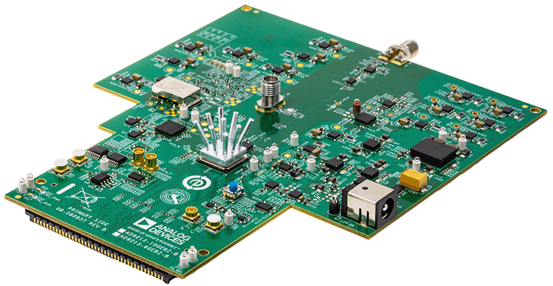
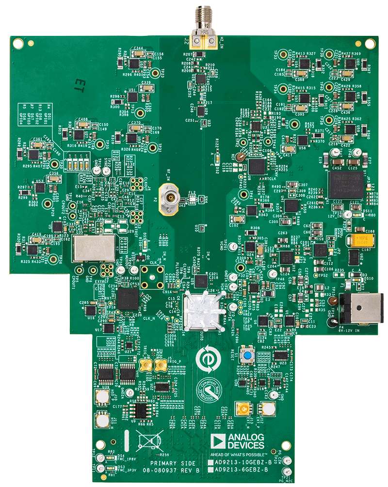
評価用キット


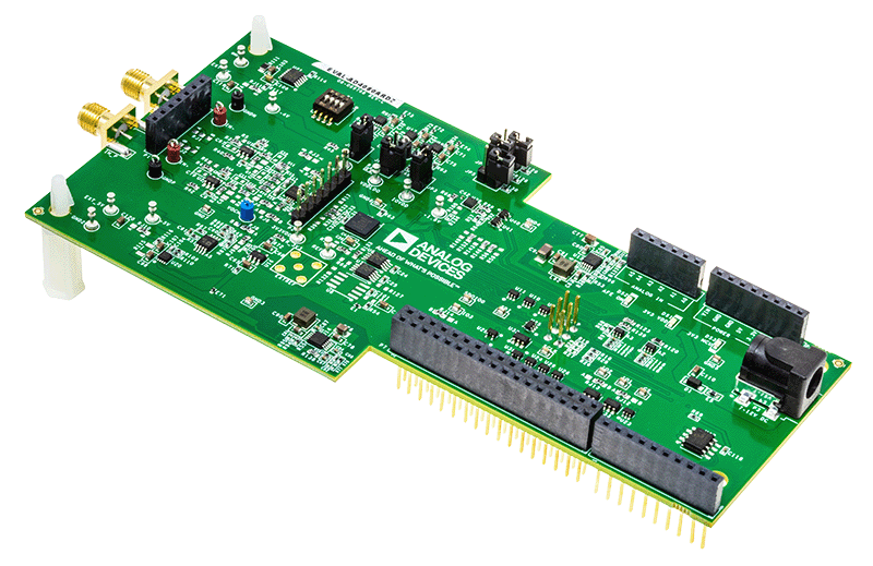
AD4083/AD4084(16ビット、40/20MSPS、差動SAR ADC)の性能評価
資料
DCカップリング10GSPSデジタイザ評価用ボード
資料
ソフトウェア


Mixed-Mode Signal Chain Active Learning Module
資料
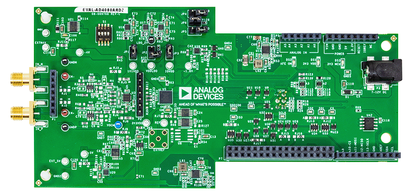
AD4080(高速、高精度の20ビット、40MSPS、差動SAR ADC)の性能評価
資料
ソフトウェア
最新のディスカッション
AD4085に関するディスカッションはまだありません。意見を投稿しますか?
EngineerZone®でディスカッションを始める