ADC Driving: Pseudo-Differential Unipolar or Bipolar Inputs
ADC Driving: Pseudo-Differential Unipolar or Bipolar Inputs
by
Guy Hoover
Aug 28 2013
For most applications, we recommend the low power LT6202 ADC driver to drive the LTC2369-18. With a low noise density of 1.9nV/√Hz and a low supply current of 3mA, the LT6202 is flexible and may be configured to convert signals of various amplitudes to the 0V to 5V input range of the LTC2369-18.
To achieve the full distortion performance of the LTC2369-18, a low distortion single-ended unipolar signal source driven through the LT6202 configured as a unity-gain buffer as shown in Figure 1 can be used to get the full data sheet THD specification of –120dB.
The noise and distortion of the buffer amplifier and signal source must be considered since they add to the ADC noise and distortion. Noisy input signals should be filtered prior to the buffer amplifier input with an appropriate filter to minimize noise. The simple 1-pole RC lowpass filter (LPF1) shown in Figure 1 is sufficient for many applications.


Another filter network consisting of LPF2 should be used between the buffer and ADC input to both minimize the noise contribution of the buffer and to help minimize disturbances reflected into the buffer from sampling transients. Long RC time constants at the analog inputs will slow down the settling of the analog inputs. Therefore, LPF2 requires a wider bandwidth than LPF1. A buffer amplifier with a low noise density must be selected to minimize degradation of the SNR.
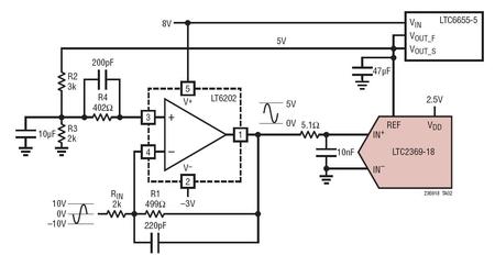
Figure 2 shows the LT6202 being used to convert a ±10V, single ended, true bipolar signal for use by the LTC2369-18. In this case, the LT6202 is configured as an inverting amplifier stage, which acts to attenuate and level shift the input signal to the 0V to 5V input range of the LTC2369-18. In the inverting configuration, the single-ended input signal source no longer directly drives a high impedance input. The input impedance is instead set by resistor RIN. RIN must be chosen carefully based on the source impedance of the signal source. Higher values of RIN tend to degrade both the noise and distortion of the LT6202 and LTC2369-18 as a system. Table 1 shows the resulting SNR and THD for several values of RIN, R1, R2, R3 and R4 in this configuration. Figure 3 shows the resulting FFT when using the LT6202 as shown in Figure 2.


| RIN (Ω) | R1 (Ω) | R2 (Ω) | R3 (Ω) | R4 (Ω) | SNR (dB) | THD (dB) |
| 2k | 499 | 499 | 2k | 402 | 96.1 | −97.3 |
| 10k | 2.49k | 2.49k | 10k | 2k | 96 | −92 |
| 100k | 24.9k | 24.9k | 100k | 20k | 93.8 | −93.5 |
About the Authors
Guy Hoover is an engineer with over 30 years of experience at Linear Technology as a technician, an IC design engineer and an applications engineer.
He began his career at LTC as a technician, learning from Bo...
He began his career at LTC as a technician, learning from Bo...
Related to this Article
Resources
Data Sheet


