Passing the Radiated Emissions Test: How to Eliminate Complex EMI Mitigation Techniques for Compact and Cost-Effective Isolated Designs
Thought Leadership
Passing the Radiated Emissions Test: How to Eliminate Complex EMI Mitigation Techniques for Compact and Cost-Effective Isolated Designs
Isolation is required for a variety of reasons in electronic systems. It is needed to protect people and equipment from high voltages, or to simply remove unwanted ground loops on a PCB. It’s an essential design element in a wide variety of applications, including factory and industrial automation, medical equipment, communications, and consumer products. While critically necessary, isolation design is also extremely complex. When controlled power and data signals are passed across the isolation barrier, it creates electromagnetic interference (EMI). These radiated emissions (RE) can negatively affect the performance of other electronic systems and networks.
While critically necessary, isolation design is also extremely complex. When controlled power and data signals are passed across the isolation barrier, it creates electromagnetic interference (EMI). These radiated emissions (RE) can negatively affect the performance of other electronic systems and networks.
An important step in circuit design with isolation is to transfer power across the isolation barrier and mitigate the resulting RE. Though conventional approaches can be effective, they often come with trade-offs. They may include the use of discrete circuitry and transformers for the transfer of power. This is a bulky, time-consuming approach that takes up valuable PCB space—all of which leads to higher costs. More cost-effective solutions integrate the transformer and required circuitry into smaller form factors, such as chip packages.
While this saves board space and reduces design complexity and cost, it results in a smaller transformer with fewer windings and the need for higher switching frequencies (up to 200 MHz) to efficiently transfer the required power to the secondary side. At these higher frequencies, parasitic common-mode (CM) currents may capacitively couple from the primary side to the secondary side through the windings of the transformer. Due to the nature of the isolation barrier, there is no physical path to return these CM currents to the primary side. The isolation barrier forms a dipole that radiates energy as the CM current and returns it to the primary side. This presents another significant consideration: regulatory compliance.
EMC Requirements
Before a product is marketed, it must conform to electromagnetic-compatibility (EMC) regulations. The integration of transformers and required circuitry into smaller packages results in EMI, which requires complex and costly RE mitigation techniques in order to meet EMC regulations.
EMC is the ability of an electronic system to function properly in its intended environment without interfering with other systems. EMC regulations exist in different global regions to ensure all products can function correctly in the presence of other products. Radiated emissions must be below a specified level based on the intended use environment and application. EMC testing and certification have therefore become an integral part of bringing a product to market. Products sold in the EU require a CE mark, while those sold in the U.S. require an FCC classification. Attaining these certifications requires a suite of EMC tests to be performed on the system. In industrial, medical, communication, and consumer environments, radiated emissions typically have to comply with CISPR 11/EN 55011, CISPR 32/EN 55032, or FCC Part 15.
CISPR 11/EN 55011
This standard applies to equipment designed to generate RF energy for industrial, scientific, and medical (ISM) purposes. Within the standard, equipment may be categorized into one of two groups. Group 2 is for all ISM RF equipment in which radio frequency energy is intentionally generated and used locally. Group 1 contains all equipment in the scope of the standard that is not classified as Group 2 equipment.
CISPR 32/EN 55032
This standard applies to information technology equipment (ITE) whose primary function is a combination of entry, storage, display, retrieval, transmission, processing, switching, or control of data and telecommunications messages, and which may be equipped with one or more terminal ports typically operated for information transfer.
Equipment is classified further within each of these standards, with each class governed by a separate set of emissions limits.
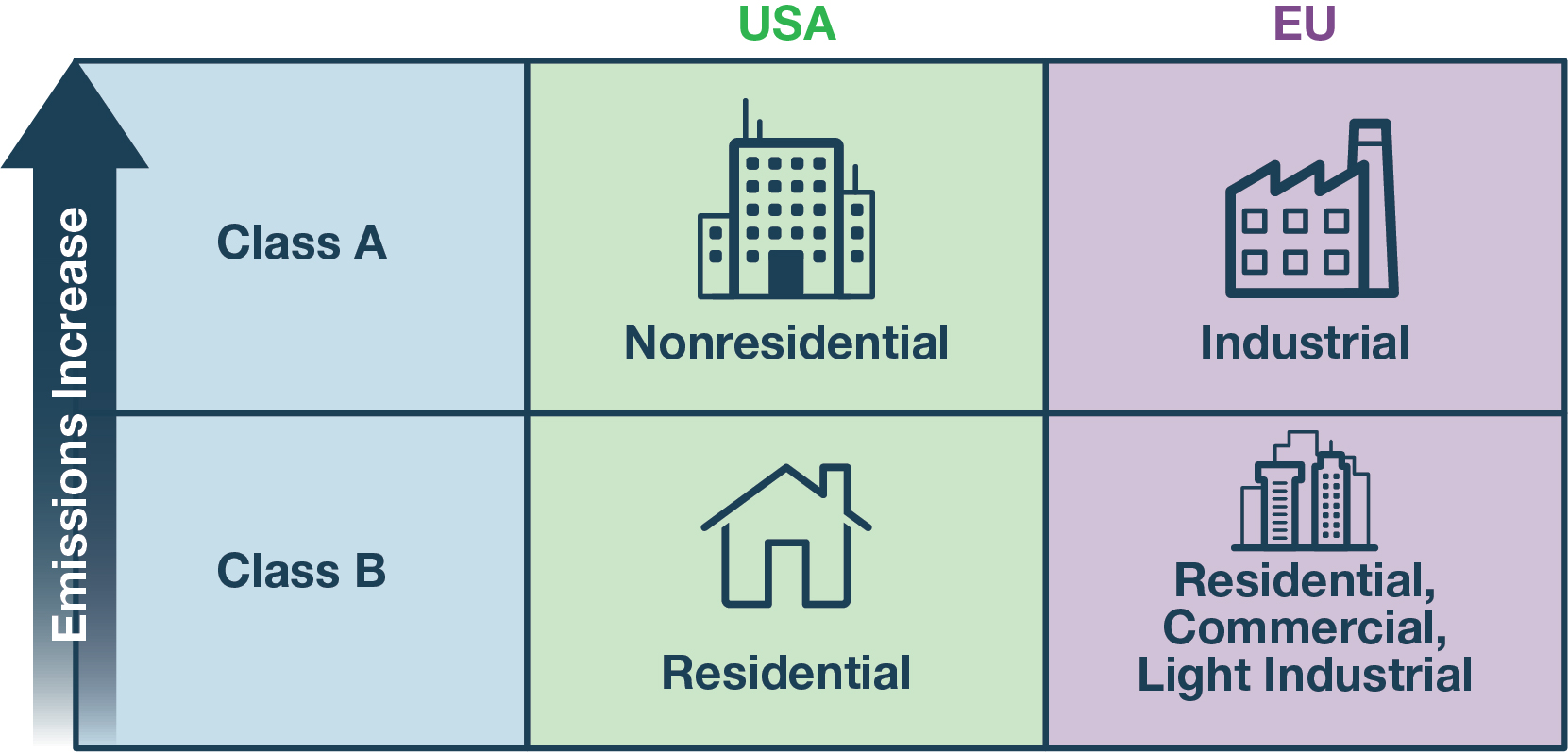
- Class A: equipment used in industrial applications and nonresidential areas
- Class B: equipment used in residential environments
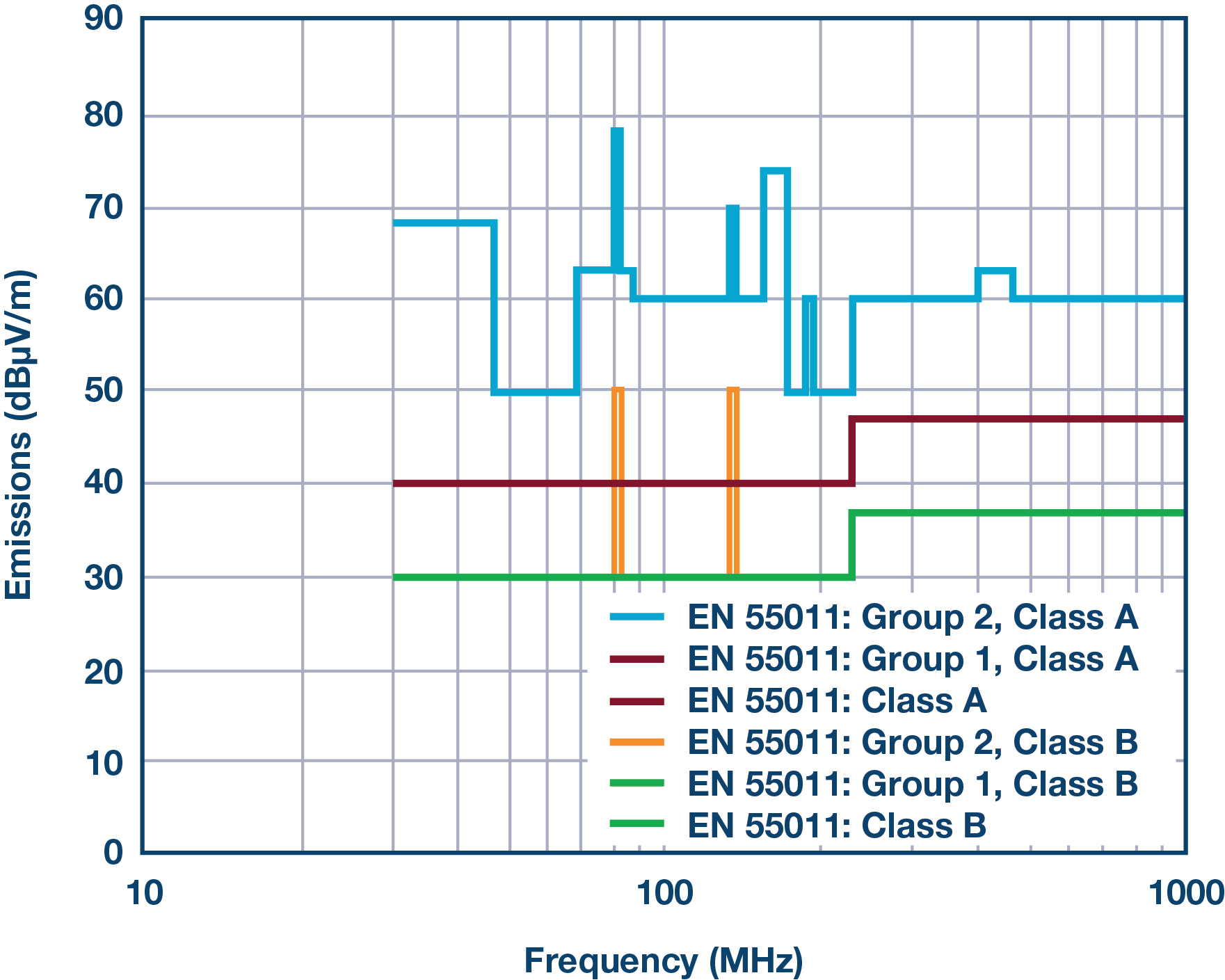
Because Class B limits cover residential (or light industrial) environments where products are more likely to be within close proximity to one another (within 10 m of broadcast radio and television receivers), they are more stringent (as much as 10 dB lower than Class A) so as not to cause interference issues.
Figure 2 shows the limit lines associated with CISPR 11/EN 55011 and CISPR 32/EN 55032 for both Class A and B. In this frequency range, compliance to CISPR 32/EN 55032 Class B implies compliance to CISPR 11/EN 55011 Class B.
Consider EMC at the Start of the Design Cycle
It has been reported that 50% of products fail EMC testing the first time.1 This may be a result of lack of knowledge and failure to apply EMC design techniques early in the product design phase. Ignoring EMC until the functional design is completed often creates a time-consuming and costly challenge. In addition, techniques available to solve EMC issues decrease as you move further along the product development path, as aspects of the product cannot be changed without schedule overruns and increased costs.
Designing for EMC at the start of your project is critical to minimizing design time and project cost. The choice and placement of components are also important. Selecting and designing in devices that already meet industry standards can increase the ability to meet compliance.
EMI Mitigation Techniques: The Need for a Better Way
Compared to conventional approaches that use discrete transformers, the integration of a transformer and circuitry into a chip scale package will lead to greatly improved PCB space-saving due to the reduction in the number of components, but may introduce higher radiated emissions. Radiated emissions mitigation techniques may negate the savings of the integrated transformer and cost due to added PCB design complexity or additional components.
For example, a common way to mitigate radiated emissions at the PCB level is to create a low impedance path from the secondary to the primary side for CM currents and therefore reduce the level of RE. This can be achieved by using a stitching capacitor between the primary and the secondary side. The stitching capacitor can be either a discrete or an embedded interlayer capacitor.
A discrete capacitor is the least complex solution and may be a leaded or surface-mount component. It also has the benefit of being suitable for a 2-layer PCB, but discrete capacitors are expensive and bulky. They also take up valuable PCB real estate, especially along the isolation barrier where multiple components may be stacked.
Another less than ideal solution is using an embedded stitching capacitor, which is formed when two planes in a PCB overlap (Figure 3). This type of capacitor has some very useful properties in that the inductance of the parallel plate capacitor is extremely low and is therefore effective over a larger frequency range. It will improve emissions performance, but it adds design complexity and cost due to customizing the layer thickness to get the correct capacitance and the requirement of four or more layers in the PCB. The spacing between internal overlapping layers must also meet minimum specifications for distance through the insulation as defined by the relevant isolation standard.

A stitching capacitor also allows ac leakage and transients to couple across the barrier from one ground plane to the other. Although the stitching capacitance is generally small, high voltage, high speed transients can inject significant currents across the barrier through this capacitance. This must also be taken into account if the application is subjected to harsh electromagnetic transients, such as electrostatic discharge, electrical fast transients, and surge.
The use of stitching capacitance, whether a discrete or embedded capacitor, is not an ideal mitigation technique. It will aid in reducing radiated emissions but at the expense of additional components, complex PCB layout, and increased transient susceptibility. Ideal mitigation techniques would not require the need for a stitching capacitance and hence improve costs and reduce PCB design complexity.
Eliminate the Need for Complex Mitigation Techniques
Ideally, an integrated isolated power component should contain measures to reduce the emissions within the chip and guarantee passing the systemlevel emissions without having to create intricate extra external measures. This will allow passing stringent emissions tests without multiple board spins just by placing the components on a simple 2-layer board.
Low Radiated Emissions Isolator
Analog Devices' next-generation isoPower® family incorporates innovative design techniques that avoid the generation of high level radiated emissions, even on a 2-layer board with no stitching capacitance. The ADuM5020 and ADuM5028 can provide 500 mW and 330 mW of power, respectively, across the isolation barrier while meeting CISPR 32/EN 55032 Class B limits with substantial margin.
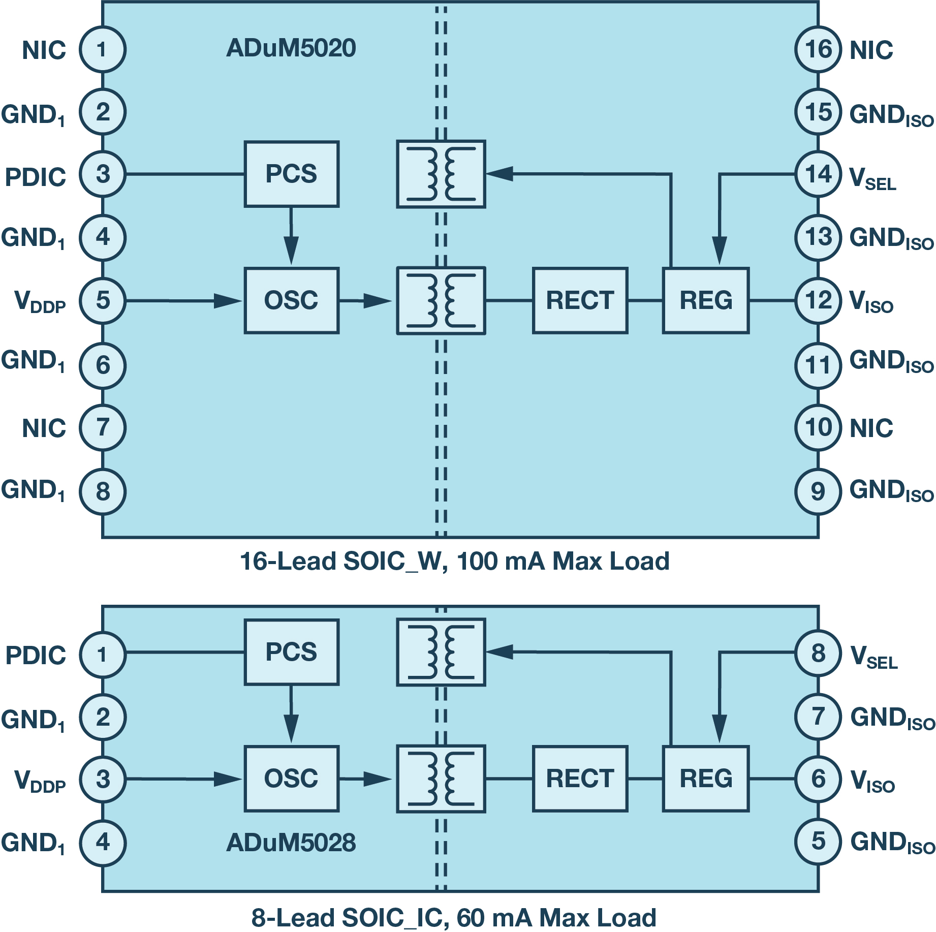
The ADuM5020 comes in a 16-lead, wide-body SOIC package, while the smallest package option is the 8-lead SOIC for the ADuM5028. The ADuM5020/ADuM5028 offers both 3 V and 5 V power supply options and an isolation rating of 3 kV rms. The ADuM5020/ADuM5028 offers 5 kV rms and meets the same power and emissions levels as the ADuM5020/ADuM5028.
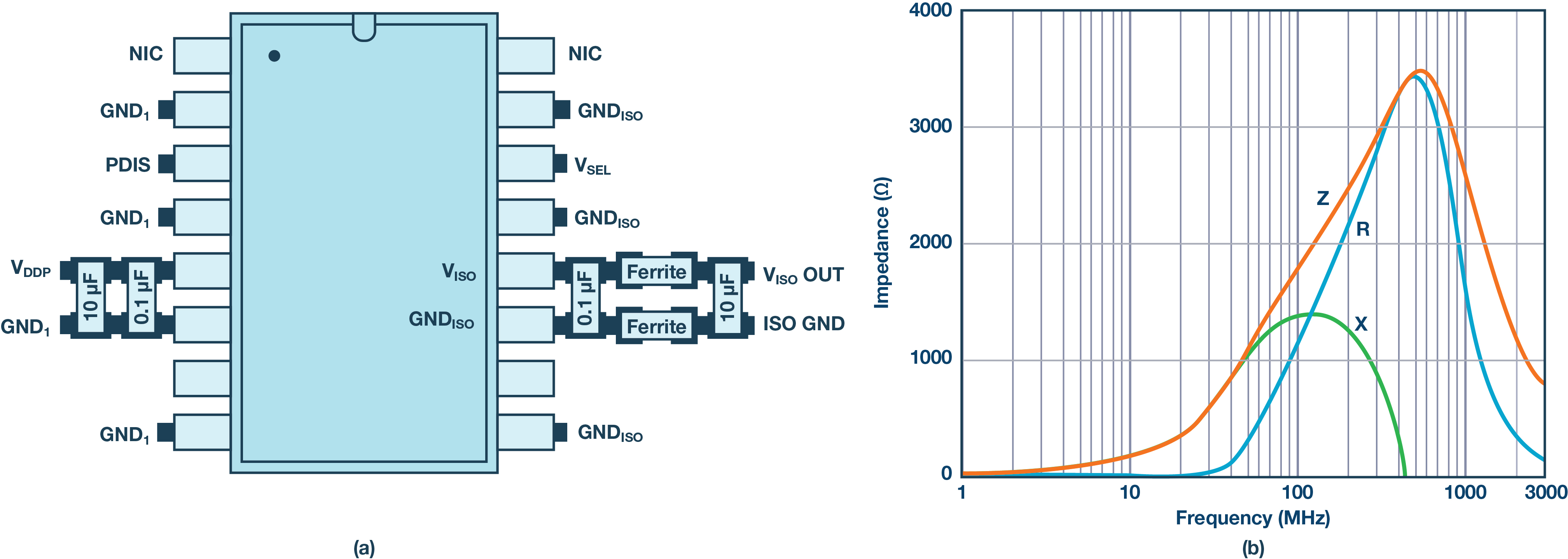
In order to reduce radiated emissions, the ADuM5020/ADuM5028 has excellent coil symmetry and coil driver circuits that help minimize the transfer of CM currents across the barrier. Spread spectrum techniques are also employed to reduce noise concentration at a particular frequency and spread the radiated emissions energy over a wider band of frequencies. The use of inexpensive ferrite beads on the secondary side further reduces emissions. These techniques improve the levels of both the peak and quasi-peak measurements during RE compliance testing.
Figure 5 shows the ferrite beads placed on the secondary side close to the VISO and the GNDISO pins. The ferrite used to gather the emission plots in the following section was the Murata BLM15HD182SN1. These ferrites have a high impedance over a wide frequency range (1800 Ω at 100 MHz and 2700 Ω at 1 GHz). With these ferrites, the effective radiation efficiency of the dipole is reduced. As shown in Figure 6, due to the impedance of the ferrite bead the effective length of the dipole is significantly shortened, leading to a less efficient dipole and reduced emissions.

The ADuM5020/ADuM5028 offers a drop-in dc-to-dc power solution. With a small footprint and excellent RE performance, it is a cost-effective, low complexity solution that will aid in meeting EMC regulations if designed into the product at the start of the design cycle.
Results from the Testing Chamber
The ADuM5020/ADuM5028 was tested in a 10 m semi-anechoic chamber according to CISPR 32/EN 55032 testing guidelines. Figure 7 shows a typical 10 m chamber. The ADuM5020/ADuM5028 evaluation PCB is placed at a distance of 10 m from the antenna calibration point on a nonconductive table, as specified in the standard. It is important that no other conductive surfaces are within proximity of the DUT, as this will affect results. Figure 8 shows a peak scan that is used to determine high emission frequencies from the DUT. With these points located, quasi-peak measurements are made. During the quasi-peak measurements, the table is rotated 360° and the antenna height is raised from 1 m to 4 m. The worst-case quasi-peak measurement is recorded and compared to the required limit lines.
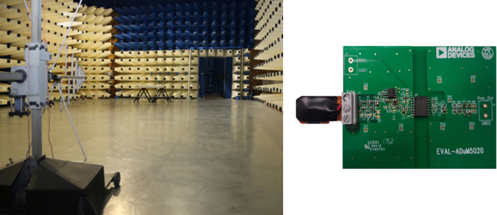
It is important that no external equipment, metal planes, or cables interfere with the emissions testing of the DUT. In order to test the ADuM5020/ADuM5028 evaluation board, a battery with an on-board low dropout regulator was used to keep the power supply current loop small and remove unnecessary cabling.
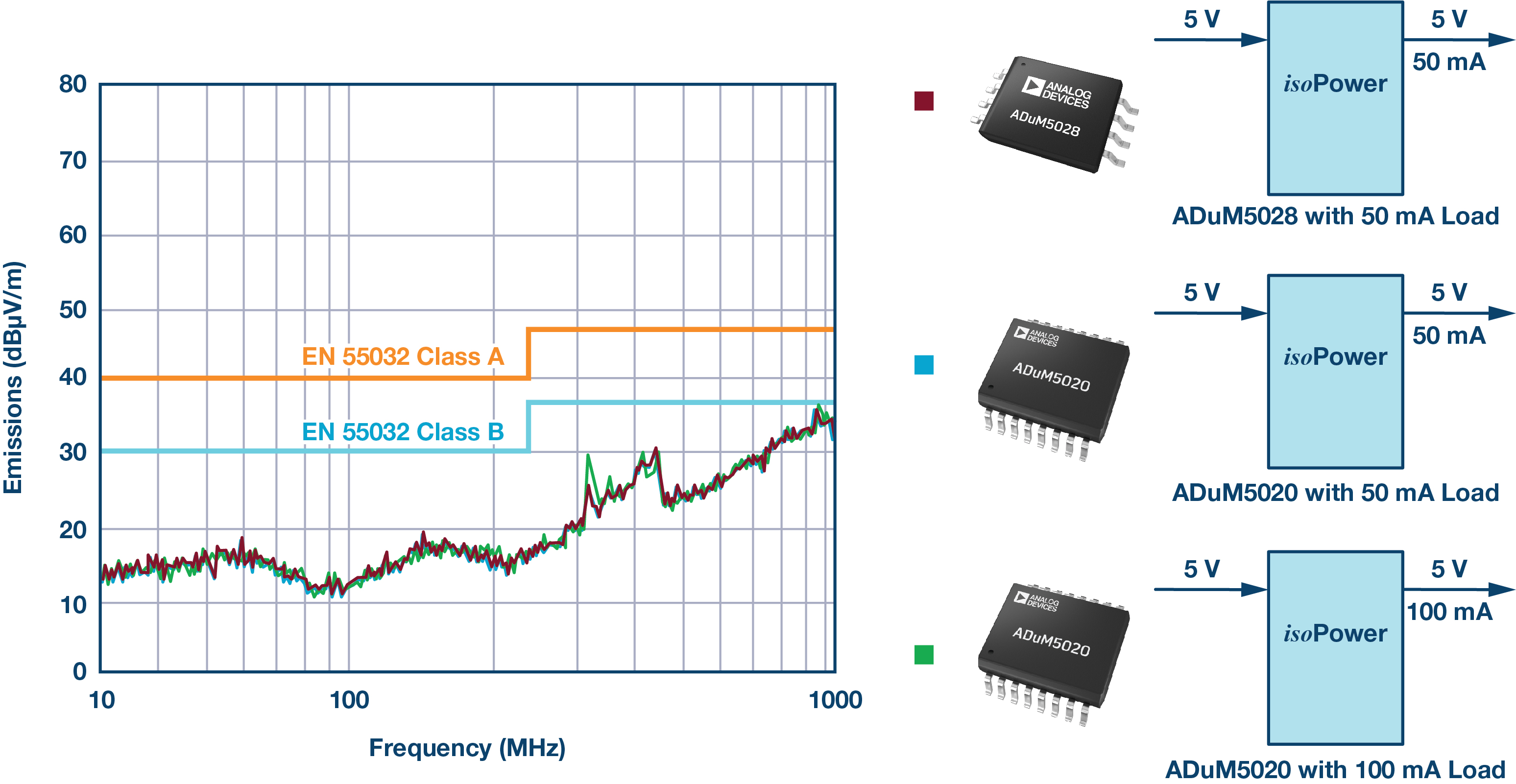
Figure 8 shows the peak plots captured for the ADuM5020/ADuM5028 in different configurations. Note the spread of energy over a wide band due to the spread spectrum techniques employed within the ADuM5020/ADuM5028. Figure 9 shows the margin of the worst-case quasi-peak measurement to CISPR 32/EN 55032 Class B limit lines. The ADuM5020 with 100 mA load at 5 V output supply (500 mW) passes CISPR 32/EN 55032 by more than a 5 dB margin. This offers a great degree of design flexibility. This degree of margin is beneficial and recommended as there may be variances in the quality of the test chamber, calibration, and accuracy of equipment in different test facilities that can lead to measurement differences. This may be of concern if the final product may be tested at different chambers and must meet CISPR 32/EN 55032.
| VIN/VISO 5 V/5 V | VISO Output Current (mA) | Worst-Case Quasi-Peak Frequency (MHz) | CISPR 32 Class B Quasi-Peak dBµV/m Class B Margin (dB) |
| ADuM5028 | 50 | 920 | Passes by –6.3 |
| ADuM5020 | 50 | 935 | Passes by –6.9 |
| ADuM5028 | 100 | 915 | Passes by –5.1 |
Analog Devices' next-generation isoPower family, offers compact, drop-in power solutions that do not require complex PCB level mitigation in order to meet emissions limits. The ADuM5020/ADuM5028 offers a dc-to-dc drop-in power solution for isolated designs that meets emissions standards set in the following emissions and product standards:
- CISPR 32/EN 55032 (Class B): Information Technology Equipment
- CISPR 11/EN 55011 (Class B): Industrial, Scientific, and Medical Equipment
- IEC 61000-6-4: Generic Standards—Emission Standard for Industrial Environments
- IEC 61000-6-3: Generic Standards—Emission Standard for Residential, Commercial, and Light-Industrial Environments
- IEC 61131-2: Programmable Controllers—Part 2: Equipment Requirements and Tests
- IEC 621326: Electrical Equipment for Measurement, Control, and Laboratory Use EMC Requirements—Part 1: General Requirements
- IEC 60601-1-2: Medical Electrical Equipment Part 1-2: General Requirements for Basic Safety and Essential Performance—Collateral Standard: Electromagnetic Disturbances—Requirements and Tests
- IEC 61800-3: Adjustable Speed Electrical Power Drive Systems— Part 3: EMC Requirements and Specific Test Methods
- IEC 63044-5-1: Home and Building Electronic Systems (HBES) and Building Automation and Control Systems (BACS)—Part 5-1: EMC Requirements, Conditions, and Test Set-Up
Reducing Complexity and Compromise in Isolation Design
Designing power for isolation can be one of the most challenging aspects of a design process. Creating a solution requires balancing design demands with the need for regulatory compliance in a number of different global regions. The result can often mean compromises that negatively affect size, weight, and performance, or that threaten the ability to meet EMC compliance.
In order to achieve EMC success, incorporate devices that are proven to meet industry standards early in the design phase. EMC should be part of the design process and not an afterthought. The use of mitigation techniques such as stitching capacitance reduce the transient immunity of the electronic system and increase cost and design complexity. Analog Devices' next-generation isoPower family offers radiated emissions mitigation techniques that remove the need for a stitching capacitor while still meeting CISPR 32/EN 55032 Class B. The ADuM5020/ADuM5028 incorporates spread spectrum techniques that reduce the level of power at any one frequency. Excellent design, transformer coil symmetry, and the use of two small, inexpensive ferrites reduce the flow of CM current across the isolation barrier and into the secondary ground plane. The ADuM5020/ADuM5028 reduces costs by meeting CISPR 32/EN 55032 Class B with significant margin on a 2-layer PCB without the need for expensive PCB level RE mitigation techniques.
References
1 “Why 50% of Products Fail EMC Testing the First Time.” Intertek.


 Close Details