Software Control of the MAX6952 and MAX6953 LED Drivers in Graphic Applications
Abstract
This application note discusses software design techniques to build monocolour and bicolour graphic message boards using the MAX6952 and MAX6953 SPI and I2C 5 × 7 matrix LED display drivers.
This application note is one of two application notes that discuss the software and processor interface issues in the application of the MAX6952 and MAX6953 LED drivers to build a sea-of-dots LED matrix graphic panel for message boards and animated graphic displays. This note covers the software aspects of the panel design. The other note, "Building LED Dot Matrix Graphic Panels with the MAX6952 and MAX6953," covers the electrical aspects of the panel design, and should be read first.
The MAX6952 and MAX6953 are 4-digit cathode-row 5×7 matrix LED display drivers that are controlled through a high-speed SPI™ (MAX6952) or I2C (MAX6953) serial interface. These drivers are primarily intended for character display applications where individual 5×7 matrix digits are physically spaced apart to form one or more character lines (Figure 1).
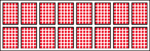
Figure 1. Example of an 8 character by 2 lines matrix display panel using 5×7 matrix characters.
The MAX6952 and MAX6953 treat 4 individual 5×7 matrix LEDs as 4 character digits. The user controls which of 104 fixed and 24 user-defined characters is displayed on each digit. The user can up-load custom characters into the 24 user-defined fonts after power-up, if required. The display is controlled using digit registers to select a character from the 128-character font. This methodology is fast and efficient for character displays, but inappropriate for graphic displays.
For graphic applications using the MAX6952 or MAX6953, the control technique is the opposite. The fixed fonts are ignored, and the 24 user-defined fonts are used for direct graphical display control. The digit registers are each set to point to a different user-defined font location, and the fonts themselves are manipulated to adjust the graphic display in 5×7 sections. If blink control isn't required, then only 4 user-defined font locations are needed, one for each 5×7 section (Table 1). 8 user-defined font locations are needed if blink is used, one for each blink phase (P1 and P0) for each 5×7 section (Table 2). The digit registers need only be written once with the appropriate RAMxx character address, and the fonts themselves are manipulated to set up the graphic image.
| Digit 0 | Digit 1 | Digit 2 | Digit 3 | |
| Font Location | RAM00 | RAM01 | RAM02 | RAM03 |
| Digit 0 | Digit 1 | Digit 2 | Digit 3 | |||||
| Blink Phase | P1 | P0 | P1 | P0 | P1 | P0 | P1 | P0 |
| Font Location | RAM00 | RAM04 | RAM01 | RAM05 | RAM02 | RAM06 | RAM03 | RAM07 |
The simple scheme outlined above is adequate for static displays, where the graphic image is uploaded relatively infrequently to the display, perhaps using blink to provide some animation effects. However, it is possible to get a high degree of artifact-free image manipulation by making full use of more of the user-defined fonts. There are 24 user-defined font locations available, and only 4 (without blink) or 8 (with blink) font locations are actually needed to store the displayed graphic image. The extra font locations can be used to pre-load graphic frames. A graphic frame is the complete display image that is stored in the display driver in order to be displayed. The 24 user-defined fonts allow the display driver to store 3 complete graphic frames (one of which being displayed) with blink control on the pixel level (Table 4), or 6 complete frames without blink control (Table 3). Pre-loading is the art of sending image data to the display drivers before it is required to be displayed.
| Digit 0 | Digit 1 | Digit 2 | Digit 3 | |
| Frame 1 Font Locations | RAM00 | RAM01 | RAM02 | RAM03 |
| Frame 2 Font Locations | RAM04 | RAM05 | RAM06 | RAM07 |
| Frame 3 Font Locations | RAM08 | RAM09 | RAM0A | RAM0B |
| Frame 4 Font Locations | RAM0C | RAM0D | RAM0E | RAM0F |
| Frame 5 Font Locations | RAM10 | RAM11 | RAM12 | RAM13 |
| Frame 6 Font Locations | RAM14 | RAM15 | RAM16 | RAM17 |
| Digit 0 | Digit 1 | Digit 2 | Digit 3 | |||||
| Blink Phase | P1 | P0 | P1 | P0 | P1 | P0 | P1 | P0 |
| Frame 1 Font Location | RAM00 | RAM04 | RAM01 | RAM05 | RAM02 | RAM06 | RAM03 | RAM07 |
| Frame 2 Font Locations | RAM08 | RAM0C | RAM09 | RAM0D | RAM0A | RAM0E | RAM0B | RAM0F |
| Frame 3 Font Locations | RAM10 | RAM14 | RAM11 | RAM00 | RAM15 | RAM12 | RAM13 | RAM17 |
The challenge to displaying dynamic images is to change the picture seamlessly without transient effects (artifacts) visible to the audience. The smaller the amount of data that has to be sent to the drivers every time the image is changed, the easier this is to achieve. A common artifact seen on message boards is scrolling ripple, because the controller cannot shift all the display data fast enough. Minimizing the data flow minimizes the processor load, and the interface data rate can be slower too.
The advantage to using the frames is that flipping the display from one pre-loaded frame to another pre-loaded frame requires fewer control words to be sent to the drivers than changing the display image itself. To change frame, the 4 digit registers of each MAX6952 or MAX6953 are written with user-defined font values corresponding with the new frame. This involves 4 writes (one write per digit register) to each MAX6952 or MAX6953. Directly changing the display image instead would involve 20 writes (5 writes each for 4 user-defined fonts) to each MAX6952 or MAX6953. Of course the frame data still has to be loaded some time, so these 20 writes to the 4 user-defined fonts still have to be performed. A good time to do this is during the power-up initialization.
The recommended technique for changing the image seamlessly requires blink to be enabled, although it is not necessary to have any blinking segments in the image. Presume for the moment that Frame 1 is in use, so the image being displayed uses RAM00 to RAM07 for Digit 0 through Digit 3 (Table 4). Note that if RAM00 data = RAM04 data, RAM01 data = RAM05 data, RAM02 data = RAM06 data, and RAM03 data = RAM07 data then the image doesn't blink because the image in blink planes P1 and P0 are the same. Another complete image can then be loaded into Frame 2, i.e., RAM08 to RAM0F. The upload can be performed as slowly or as fast as the microprocessor allows, because the image is not being displayed yet. The trick here to flip the display seamlessly from Frame 1 to Frame 2 is to change the digits' P0 data during the P1 blink phase, and then change the digits' P1 data during the P0 blink phase. The current blink phase can be monitored either on the Blink output pin, or by reading the status of the P bit in the configuration register. Note that the blink timing now sets the response time for changing the image, since an image update is synchronized to blink. If the application will use segment blinking, then weigh the competing requirements of a visibly slow segment blink speed, versus a reasonably fast response time when flipping between different images. The blink speed setting controls both these parameters.
Using frames also makes slow speed animation easy. The MAX6952 or MAX6953 drivers can store 6 frames of an animation. Again, the technique is to change the digit data for the P0 blink phase while the P1 phase is being displayed, and change the digit data for the P1 blink phase while the P0 phase is being displayed (Table 6). Segment blinking isn't used for animation, so the blink speed simply sets the animation speed or frame rate. This can be set from 4 frames a second (OSC = 8MHz) to one frame every 2 seconds (OSC = 1MHz).
The user actions in Table 5 ensure the next blink phase displays a new frame, circulating around the six available frames. The sequence therefore controls a 6 step animation, which repeats indefinitely. The animation could step through fewer than 6 frames if required; for example, the drivers could store two 3-step animations. Note that the time synchronization of successive frames is entirely set by the MAX6952 or MAX6953 drivers' blink clock. The user's task is simply to write 4 words of digit data to each MAX6952 or MAX6953 driver during each blink phase to control the animation. Not shown in Table 5 is the one-time task to upload all the frames of the animation data into the user-defined fonts of all the MAX6952 or MAX6953 drivers.
| Digit 0 | Digit 1 | Digit 2 | Digit 3 | Blink Phase | Blink Output Pin Level (Configuration register P bit) (During Current Blink Phase) |
User Action During Current Blink Phase |
|
| Initialization | Write animation data to RAM00 - RAM17 | ||||||
| Frame 1 | RAM00 | RAM01 | RAM02 | RAM03 | P0 | High | Write 0x04 to address 0x40 (Digit 0 P1) Write 0x05 to address 0x41 (Digit 1 P1) Write 0x06 to address 0x42 (Digit 2 P1) Write 0x07 to address 0x43 (Digit 3 P1) |
| Frame 2 | RAM04 | RAM05 | RAM06 | RAM07 | P1 | Low | Write 0x08 to address 0x20 (Digit 0 P0) Write 0x09 to address 0x21 (Digit 1 P0) Write 0x0A to address 0x22 (Digit 2 P0) Write 0x0B to address 0x23 (Digit 3 P0) |
| Frame 3 | RAM08 | RAM09 | RAM0A | RAM0B | P0 | High | Write 0x0C to address 0x40 (Digit 0 P1) Write 0x0D to address 0x41 (Digit 1 P1) Write 0x0E to address 0x42 (Digit 2 P1) Write 0x0F to address 0x43 (Digit 3 P1) |
| Frame 4 | RAM0C | RAM0D | RAM0E | RAM0F | P1 | Low | Write 0x10 to address 0x20 (Digit 0 P0) Write 0x11 to address 0x21 (Digit 1 P0) Write 0x12 to address 0x22 (Digit 2 P0) Write 0x13 to address 0x23 (Digit 3 P0) |
| Frame 5 | RAM10 | RAM11 | RAM12 | RAM13 | P0 | High | Write 0x14 to address 0x40 (Digit 0 P1) Write 0x15 to address 0x41 (Digit 1 P1) Write 0x16 to address 0x42 (Digit 2 P1) Write 0x17 to address 0x43 (Digit 3 P1) |
| Frame 6 | RAM14 | RAM15 | RAM16 | RAM17 | P1 | Low | Write 0x00 to address 0x20 (Digit 0 P0) Write 0x01 to address 0x21 (Digit 1 P0) Write 0x02 to address 0x22 (Digit 2 P0) Write 0x03 to address 0x23 (Digit 3 P0) |
To run a continuously changing animation sequence, more work is required by the system processor (Table 6). The user action during each frame now includes updating the font RAM for each MAX6952 or MAX6953 because the frame data is ever-changing, not stored permanently (once) as before. However the time synchronization of successive frames is still controlled by the MAX6952 or MAX6953 drivers' blink clock. The processor, again, simply has to deliver a packet of data sometime within each blink phase. The packet contains 4 words of digit data as before, plus 20 words of font data.
It is worth exploring the size limits for a graphic display when limited by the interface speed (Table 7). The table shows theoretical maximum display size with the serial interface running continuously at maximum bit rate running a continuous animation sequence. The practical limit will be at least a little (or maybe a lot) lower than the theoretical limit, depending on the background processing that the processor has to perform, and whether the serial interface is a hardware synchronous serial port or bit-banged I/O.
| Digit 0 | Digit 1 | Digit 2 | Digit 3 | Blink Phase | Blink Output Pin Level (Configuration register P bit) (During Current Blink Phase) |
User Action During Current Blink Phase |
|
| Initialization | Write animation data to RAM00 - RAM17 | ||||||
| Frame 1 | RAM00 | RAM01 | RAM02 | RAM03 | P0 | High | Write 0x04 to address 0x40 (Digit 0 P1) Write 0x05 to address 0x41 (Digit 1 P1) Write 0x06 to address 0x42 (Digit 2 P1) Write 0x07 to address 0x43 (Digit 3 P1) Ensure RAM04-RAM07 is updated for Frame 2 Can update RAM08-RAM17 if processor time and frame data are available |
| Frame 2 | RAM04 | RAM05 | RAM06 | RAM07 | P1 | Low | Write 0x08 to address 0x20 (Digit 0 P0) Write 0x09 to address 0x21 (Digit 1 P0) Write 0x0A to address 0x22 (Digit 2 P0) Write 0x0B to address 0x23 (Digit 3 P0) Ensure RAM08-RAM0B is updated for Frame 3 Can update RAM0C-RAM17, RAM00-RAM03 if processor time and frame data are available |
| Frame 3 | RAM08 | RAM09 | RAM0A | RAM0B | P0 | High | Write 0x0C to address 0x40 (Digit 0 P1) Write 0x0D to address 0x41 (Digit 1 P1) Write 0x0E to address 0x42 (Digit 2 P1) Write 0x0F to address 0x43 (Digit 3 P1) Ensure RAM0C-RAM0F is updated for Frame 4 Can update RAM10-RAM17, RAM00-RAM07if processor time and frame data are available |
| Frame 4 | RAM0C | RAM0D | RAM0E | RAM0F | P1 | Low | Write 0x10 to address 0x20 (Digit
0 P0) Write 0x11 to address 0x21 (Digit 1 P0) Write 0x12 to address 0x22 (Digit 2 P0) Write 0x13 to address 0x23 (Digit 3 P0) Ensure RAM10-RAM13 is updated for Frame 5 Can update RAM14-RAM17, RAM00-RAM0Bif processor time and frame data are available |
| Frame 5 | RAM10 | RAM11 | RAM12 | RAM13 | P0 | High | Write 0x14 to address 0x40 (Digit
0 P1) Write 0x15 to address 0x41 (Digit 1 P1) Write 0x16 to address 0x42 (Digit 2 P1) Write 0x17 to address 0x43 (Digit 3 P1) Ensure RAM14-RAM17 is updated for Frame 6 Can update RAM00-RAM0F if processor time and frame data are available |
| Frame 6 | RAM14 | RAM15 | RAM16 | RAM17 | P1 | Low | Write 0x00 to address 0x20 (Digit
0 P0) Write 0x01 to address 0x21 (Digit 1 P0) Write 0x02 to address 0x22 (Digit 2 P0) Write 0x03 to address 0x23 (Digit 3 P0) Ensure RAM00-RAM03 is updated for Frame 1 Can update RAM04-RAM13 if processor time and frame data are available |
| Mono-color 40x56 pixel sub-block (16 MAX6952/3 drivers) |
Bi-color 40x56 pixel sub-block (32 MAX6952/3 drivers) |
|||
| Simple Animation 4 words per driver per frame |
Full Animation 24 words per driver per frame |
Simple Animation 4 words per driver per frame |
Full Animation 24 words per driver per frame |
|
| I2C Interface bits/frame | 18 × 4 × 16 = 1152 bits | 18 × 24 × 16 = 6912 bits | 18 × 4 × 32 = 1304 bits | 18 × 24 × 32 = 13824 bits |
| SPI Interface bits/frame | 16 × 4 × 16 = 1024 bits | 16 × 24 × 16 = 6144 bits | 16 × 4 × 32 = 2048 bits | 16 × 24 × 32 = 12288 bits |
| 400k bits-1 I2C Interface maximum display size | 342 sub-blocks | 57 sub-blocks | 171 sub-blocks | 28 sub-blocks |
| 26M bitss-1SPI Interfacemaximum display size | 25200 sub-blocks | 4200 sub-blocks | 12600 sub-blocks | 2100 sub-blocks |
The SPI interface is likely to be the preferred interface for all but the smallest display size. Each I2C MAX6953 can be set to one of 16 I2C addresses. This means that each mono-color sub-block comprising 16 MAX6953s must be run on its own I2C bus to avoid addressing conflicts. A moderate size graphic display with, say, 224 × 80 pixels would use 6 mono-color sub-blocks requiring 12 processor I/O lines to handle the 6 I2C buses. The same panel could be driven instead by 2 processor I/O lines if the SPI MAX6952s were used daisy-chained (cascaded SPI interface) instead.
Using MAX6952s, the limiting display size is 2100 sub-blocks for a bi-color panel with full animation. A practical design example may have a processor than can devote a quarter of its time to the interface, running at 10 Mbits-1 (over an RS-485 link). The display size limit therefore drops to (2100 × 10/26 × 1/4) = 200 sub-blocks for this application. The largest bi-color panel that can be driven is therefore 10 sub-blocks by 20 sub-blocks, perhaps arranged as 1120 × 400 bi-color pixels. A mono-color panel twice this size could be driven instead.


