Seven Steps To Successful Ultralow Light Signal Conversion
The photodiode remains the basic choice for photo detection among solid-state detectors (Figure 1). It is widely used in optical communication and medical diagnosis. Other applications include color measurement, information processing, barcodes, camera exposure control, e-beam edge detection, faxes, laser alignment, aircraft landing aids, and missile guidance.
The energy transmitted by light to one of these sensors generates a current that is further processed using a high precision preamplifier. Analog-to-digital conversion and digital signal processing form the rest of a complete signal chain. The process of selecting a sensor and designing an analog front end can be reduced to seven steps:
- Describe the signal to be measured and the design goals.
- Select the right sensor and describe its electrical output.
- Determine the maximum gain you can take.
- Identify an optimal amplifier for the preamplifier stage.
- Design the complete sensor and preamplifier gain block.
- Run a simulation.
- Take extra care when building hardware and validate.
Step 1: Signals and Goals
Based on the equivalent circuit in Figure 1, the output current is given by:

To convert the light to an electrical signal for further processing, one needs to know the ac and dc characteristics of the light source, its signal magnitude, the desired measurement resolution, and the available power supplies in the system. Knowing the magnitude of the signal’s characteristic and noise level provides clues as to how to select a sensor, what gain is necessary in our gain block, and what input voltage range and noise levels might be needed when selecting an analog-to-digital converter (ADC).
Assume that we have a light source that emits pulses of lights at 1 kHz with 50 pW to 250 nW (0.006 lux) at room temperature. This is a very low amount of light, requiring a very precise signal conditioning and signal processing chain. The object is to capture and process this signal with 16 bits of resolution and accuracy. Achieving that resolution implies the need to measure accurately to 3.8 pW.
Additionally, assume that there are +12 V and –12 V supplies available in the system. With this information, a designer should be able to calculate the signal-to-noise ratio (SNR) and design the circuitry.
Step 2: Sensor Selection
Photodiodes are usually optimized during the design process for use in either “photovoltaic” mode or “photoconductive” mode. Responsivity, which is the ratio of the detector output to the detector input, is a key parameter of the photodiode. It’s given in units of ampere/watt or volt/watt.
Large area indium gallium arsenide (InGaAs) photodiodes, which are used for instrumentation and sensing applications, have better responsivity in the region of 600 nm to 800 nm than the high speed photodiodes that are used for high speed analog and digital communication systems, instrumentation, and sensing applications.
In the absence of light, applying a voltage to a shorted circuited photodiode causes a current, IS, to flow. Illuminating the diode causes a counter current, Ilight, proportional to light intensity. Total current, ISC, is:

In Equation 2, the second and third terms limit the linearity of ISC but become negligible over quite a wide range. As a practical matter, ISC is extremely linear with respect to the incident light level and can be approximated as in:

To detect a small amount of light, the designer must specify a large area photodiode in which the minimum anticipated emitted light times the responsivity generates a current greater than the dark current of the photodiode. This will result in a signal that is above the noise floor of the photodiode sensor. For a silicon photodiode with a light wavelength greater than 1100 nm, responsivity typically is less than 0.7 A/W. Table 1 in the Hamamatsu S1336 was selected for this example.
The expected current from the photodiode can be calculated from the expected optical power from the light source in:

If the light source expends all of its energy on the active area of the chosen photodiode, then Equation 4 is the only calculation required. To get a 16-bit conversion, it is necessary to resolve to one half of a least significant bit (LSB), or 0.95 pA.
The active area of the Hamamatsu photodiode is 5.7 mm2 and has a circular pattern. It then may be necessary to use fiber cable between the sensor and the light source. Fiber optical cable may have an area larger than our photodiode. Normally, the optical power in this case is measured in W/cm2. Expressing the area of the photodiode in cm2, the result is 57 × 10–3 cm2. For the same 25 pA output current from a light source measured in W/cm2, the necessary power would be as shown in:

A silicon photodiode’s noise characteristics determine the lower limit of light detection. Looking at the photodiode’s equivalent circuit in Figure 1, there are three noise sources that are captured in:
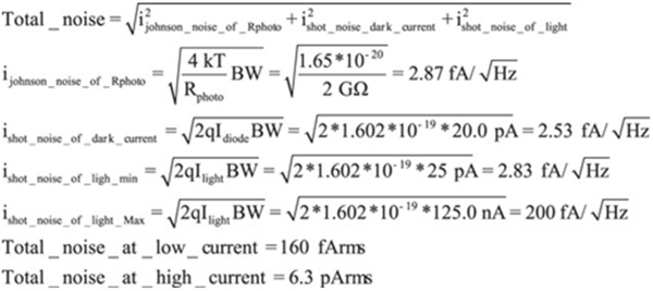
The noise of the diode is the thermal noise generated by the shunt resistance of the diode.
Step 3: Gain Block Calculations
The preamplifier extracts the small signal generated by the sensor in the presence of the larger background noisy environment. There are two types of preamplifiers for photoconductors: voltage mode and transimpedance (Figure 2).
The preamp is the first step in extracting the small signal generated by the sensor from the background noise. There are three possible configurations for interfacing a photodiode to a transimpedance amplifier. The transimpedance amp configuration in Figure 2c provides precision linear sensing from the photodiode through “zero biasing.” In this configuration, the photodiode sees a short across its output, and there is essentially no “dark” current, per Equation 3 (ISC = Ilight).
The ideal relationship (gain) between the output voltage and the input current of an I/V (transimpedance) converter can be expressed as:
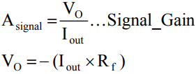
The feedback resistor value used defines the gain (sometimes called sensitivity) of the converter. For the current-to-voltage gain to be very high, Rf is made as large as other constraints permit. The designer should pick a resistor large enough to allow the minimum current out of the sensor sufficiently measureable without allowing the maximum current to saturate the amplifier.
At higher resistance values, this resistor also begins to develop significant thermal dc-voltage drift, as reflected by the temperature coefficient of the amplifier input current. To compensate for this error, an equal resistance is commonly placed in series with amplifier noninverting input and capacitively bypassed to remove most of its noise. To maximize signal-to-noise ratio, multistage gain should be avoided.
As resistor values get higher, their tolerance and temperature ratings decrease drastically. For example, it’s simple to find a 1 kΩ resistors with 0.01% tolerance but very hard and expensive to find a 10 MΩ resistor with the same tolerance.
To solve this problem, use low value resistors in series to build a larger resistance value, use low value resistors combined with multistage gains, or use “T network” circuits. Unfortunately, balancing these advantages, using largefeedback resistors tends to create errors and possible instability issues. These are addressed later in the article.
Meanwhile, this design example employs a very large value resistor: Rf = 80 MΩ. This should convert our minimum and maximum photodiode currents to more measureable output voltages as in:
Step 4: Identify an Optimal Amplifier for the Preamplifier Stage
When the photodiode is exposed to light and the circuit in Figure 2c is used, the current will flow into the inverting node of the op amp, as illustrated in Figure 3. The theoretical short-circuit situation across the photodiode occurs when the load it sees (RL) is 0 Ω and VOUT = 0 V. In reality, neither of these conditions exist in an absolute sense. RL is equal to Rf/Aopen_loop_Gain and VOUT is the virtual ground applied by the amplifier’s feedback configuration.
When a voltage is applied to a short-circuited photodiode in the absence of light, the so-called “dark current” is generated. Therefore, the amplifier must have a very large open-loop gain, and the designer must create the best “virtual ground” possible. This means very little error between the inputs of the amplifier. The deviation from 0 V across Rphoto creates an error current caused by the amplifier’s non-idealities. These sources of error are apparent in:

This requires an amplifier that introduces the least amount of these errors. In other words, the designer must pick an amplifier whose output has no more than 2 mV of error when configured with Rf = 80 MΩ in its feedback. It is also necessary to ensure the rise and fall times of the amplifier are less than the rise and fall times of the exciting laser diode source.
A few other amplifier parameters that improve the accuracy in this design that are not captured in Equation 9 are:
- Low offset voltage drift with temperature
- Low input bias current drift with temperature
- High input impedance
- Low input capacitance
- Low input current noise density
- Wide bandwidth
Pricing, package size, and power consumption are the secondary considerations in selecting the right amplifier.
The practical relationship between the output voltage and the input current of an I/V converter as stated is the gain of the converter, given by:
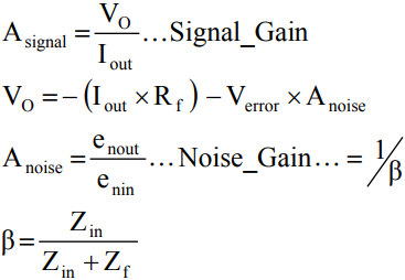
As can be seen, there is an error term in the VO equation that must be reduced as much as possible. By selecting an amplifier, that has, for example, a very large aO, then the aοβ term is increased and 1/aοβ is reduced. This will make the error term smaller.
In the example, we select the AD8627, which is a precision op amp with very low noise, low bias current, and wide bandwidth that can operate at ±12 V. The data sheet characteristics for the AD8627 are IB = 1 pA, ft = 5 MHz, en = 16 nV/√Hz at f = 1 kHz, Ccom =3.8 pF, and Cdiff = 4.1 pF. IC manufacturers have online search and selection tools to help with part selection based on user requirements. Table 2 lists a few more suitable amplifiers for light photovoltaic sensing.
|
Part Number |
VOS (µV) | IB(pA) |
UG BW (MHz) | Noise (nv/rtHz) | Package |
| AD8610/AD8620 | 100 | 10 | 25 | 6 | MSOP |
| ADA4610-2 | 400 | 25 | 9.3 | 7.3 | MSOP |
| AD8625/AD8626/AD8627 | 750 | 1 | 5 | 16 | SC-70 |
| AD8641/AD8642/AD8643 | 750 | 1 | 3.5 | 27 | SC-70 |
STEP 5: Gain Block
When the photodiode is connected to the amplifier in the configuration in Figure 2c, the amplifier very often oscillates. As noted, a large value resistor in the amplifier feedback may create abnormal behavior and oscillation. The designer must ensure the amplifier choice is the right one and that its operation when combined with the sensor is stable.
The performance of the circuit, in terms of response or bandwidth, peaking or overshoot, and noise or SNR, can get very complicated, nonlinear, and highly dependent on interactions between the active and passive elements in the converter circuit. An alternative circuit model can be used to derive a more realistic and practical analysis (Figure 4). By accounting for all of the non-idealities of this solution, Figure 4 enables the designer to perform modeling, use pole/zero analysis, and avoid problems that may arise in the future.
Interaction between the large feedback resistor and the input capacitance will introduce a zero into a pole/zero stability analysis. If Cphoto is sufficiently large, the closed-loop phase shift will approach −180° at the crossover frequency where open-loop transimpedance gain crosses the noise-gain function (Figure 5).
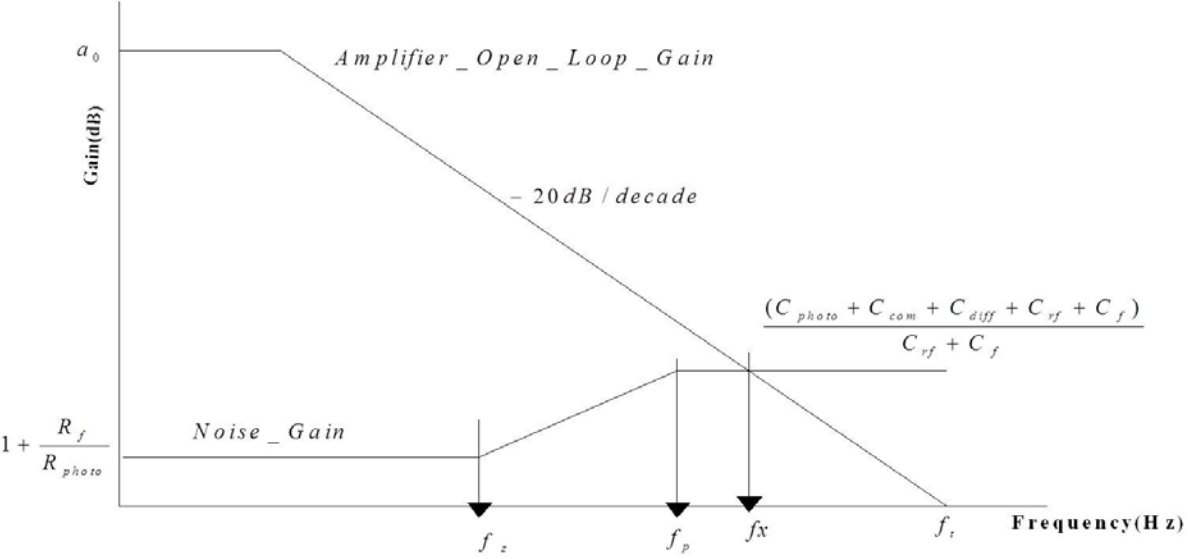
To maintain a 45° phase margin and stability, a small capacitor is needed in parallel with Rf in the feedback. The value of this capacitor is related to the input capacitance seen at the input of the amplifier. An amplifier that has a very small input capacitance makes the value of Cf smaller. When a smaller Cf is used in the circuit, more bandwidth of the amplifier is going to be used for the application on hand.
Bandwidth and sensitivity are directly traded off against each other via the selection of Rf. The example photodiode with Cphoto= 20 pF and Rf = 80 MΩ will have a maximum bandwidth of 1 kHz when the feedback capacitor (Cf = 2 pF) is placed in parallel with Rf.
Alternatively, if a 10 kHz bandwidth were required, then the designer could have picked the maximum value of Rf = 8 MΩ, and the capacitance of Cf could still be 2 pF. This concept can be useful in designing a programmable bandwidth to process different input signals, for example, at 1 kHz and 10 kHz.
The designer should run bandwidth and noise analysis to confirm that the amplifier selected is the right part for the design. The importance of picking AD8627 for its low input capacitance and bandwidth can be understood by deriving:

It can be seen that in choosing a large area photodiode, where Cphoto has a high value, fx is a lot smaller (i.e., lower bandwidth). One possible remedy to this is to pick an amplifier that has a very wide bandwidth (ft). However, that introduces other issues, such as more noise.
The amplifier, the AD8627 in this case, must have very low voltage noise to achieve low total noise in a large area photodiode, transimpedance amplifier application. It’s needed because the transimpedance circuit’s noise gain, which applies to voltage noise and resistor noise but not to the current noise, rises dramatically with frequency (noise gain = 1 + Zf/Xc). This is shown in Equation 12, where the total noise above 0.01 Hz for an I/V converter in combination with a photodiode is calculated:
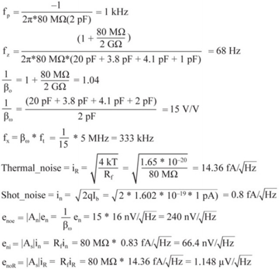
Assume that the AD8627 (IB = 1 pA, ft = 5 MHz, en = 16 nV/√Hz at f = 1 kHz, Ccom = 3.8 pF, Cdiff = 4.1 pF) is used along with that Hamamatsu photodiode (Rphoto = 2 GΩ, Cphoto = 20 pF). Additionally, Rf = 80 MΩ, Cfeedback = Crf + Cf = 2 pF. Based on the above information, the input capacitance is Cin = Cphoto + Ccom + Cdiff = 20 pF + 3.8 pF + 4.1 pF = 28 pF.
The I/V circuit’s noise gain is dominated by en, whereas the noise gains for in and iR coincide with the signal gain (Figure 6). The dominant noises are enoe in the vicinity of fx and the thermal noise, enoR, in the vicinity of fp.
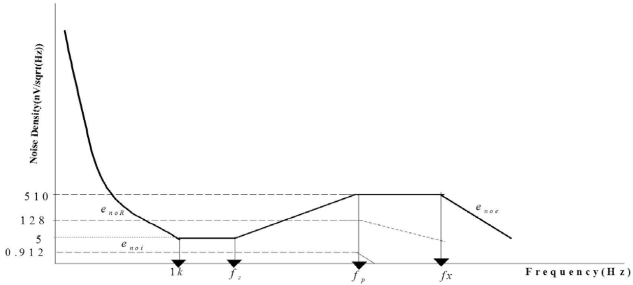

Current noise is nearly negligible because the design uses a JFET input amplifier.
Step 6: Simulation
Photodiode manufacturers do not provide Spice models for their products. However, amplifier Spice models are available for download from the the Analog Devices website. Designers can also download a free version of the popular Spice simulation software, MultiSim™,from National Instruments, from the Analog Devices site.
This software environment provides a LabVIEW® transimpedance model for a photodiode that allows customization to the specific photodiode that has been used in this design example (Figure 7a). It is important to run thorough simulation prior to building any boards. Instability may arise due to the zero introduced in the
A National Instruments MultiSim user interface to an Analog Devices model of the example transimpedance amplifier is populated with the characteristics of the Hamamatsu photodiode to enable further analysis (Figure 7a). A MultiSim simulation illustrates the instability caused by the zero introduced in the noise gain path (Figure 7b). Varying the capacitance across the feedback resistor affects usable bandwidth (Figure 7c).
As was alluded to earlier, this zero must be cancelled by introducing a pole by placing a 2 pF capacitor across the feedback resistor. The 2 pF feedback capacitance is a theoretical value. It’s possible to analyze the effects of different values on the usable bandwidth of the designed circuit (Figure. 7c). It’s also possible to validate circuit bandwidth by monitoring the output, which has −3 dB bandwidth of 1 kHz.
Step 7: Hardware Validation
Ultralow light detection circuits require discipline and the exercise of good practice in reducing all noise sources, including electromagnetic noise from the environment and all leakage sources, in addition to using very clean power supplies. It’s possible to use batteries for low voltage applications, but well bypassed power supplies using an RC or LC filter would be needed for them.
Other factors critical to success include a circuit board made from materials with high insulation resistance. To prevent leakage from getting into measurement circuitry, Guard rings or Teflon® standoffs must be used for aerial-wiring the photodiode pins to the op amp input terminals. The same is true for the feedback resistor and capacitor.
Shielded cables and a metal shielded box for the circuit are good measures against electromagnetic interference (EMI). In advanced cases, the designer can use optical fiber between the light source and photodiode.
At Analog Devices, we designed this example circuit for a range of 25 pA to 125 nA. Any signal beyond this range would saturate the amplifier and affect the overall performance. If wider range is needed, a low-leakage switch could be placed in series with the feedback resistor. Other feedback circuitries could then be used with a different sensitivity.
About the Authors
Related to this Article
Products
Precision, Low Input Bias Current, Wide BW JFET Single Op Amp
Low Input Bias Current, Wide BW JFET Precision Dual Op Amp
Precision, Low Power, Single-Supply, JFET Amplifier
Low Noise, Precision, Rail-to-Rail Output, JFET Dual Op Amp
Low Power, Rail-to-Rail Output, Precision JFET Quad Amplifier
Low Power, Rail-to-Rail Output, Precision Dual JFET Op Amp
Low Power, Rail-to-Rail Output Precision Single JFET Op Amp
Precision, Low Power, Single Supply JFET Amplifier in 5-Lead SC70
Precision, Low Power, Single-Supply, JFET Amplifier in MSOP


