LVDS Enables High-Speed Signal Distribution in 3G Base Stations
Abstract
This application note discusses use of the EIA/TIA-644 low-voltage differential signaling (LVDS) standard in 3G mobile communications. Offering both low power and a low emission, LVDS is ideally suited for high-speed clock and signal distribution in WCDMA, EDGE and cdma2000® base stations. The MAX9205 serializer, MAX9206 deserializer, MAX9150 multiport repeater, and MAX9152 crosspoint switch are featured.
A similar version of this article appeared in the July 1991 issue of Wireless Design and Development magazine.
Introduction
3G mobile communications, such as WCDMA, EDGE, and cdma2000, promise media-rich, high-speed Internet access using cell phones and other wireless communication devices. Cellular base stations connect wireless handsets to the wireline networks. To provide the bandwidth for these new applications, base stations will need to process and distribute exponentially greater amounts of digital data.
Inside the base station, data moves at high speeds across backplanes, through cables, and within circuit boards. Low-voltage differential signaling (LVDS) is a signaling standard of choice for delivering this data while minimizing space, noise, and power.
This application note discusses data and clock distribution applications using LVDS serializers, deserializers, multiport repeaters, crosspoint switches, and level translators. The focus is on the LVDS circuits, architectures, and specifications that are most relevant to 3G base-station design.
LVDS Basics for Base Stations
LVDS is a physical layer data-interface standard defined by the TIA/EIA-644 and the IEEE® 1596.3 standards. It is designed for high-speed, low-power, and low-noise point-to-point communications, typically over balanced, controlled-impedance media of 100Ω. Similar to other differential signaling standards, LVDS radiates less noise than single-ended signals due to the canceling of magnetic fields; it is more immune to noise because it is coupled onto the two wires as a common-mode signal (i.e., equal levels of noise appear on both lines). In addition, LVDS drivers use a current-steering output configuration (Figure 1) that reduces ground bounce and eliminates shoot-through current compared with voltage-mode drivers used in other differential-signaling standards. Reduced voltage swing (only ±350mV versus ±800mV for positive-referenced emitter-coupled logic, PECL, and ±2V for RS-422) allows LVDS to achieve data rates comparable to PECL (> 800Mbps) while dissipating only one-tenth the power. This combination of high-speed, low-power, and low-noise makes LVDS the ideal signaling standard for distribution in 3G base stations.
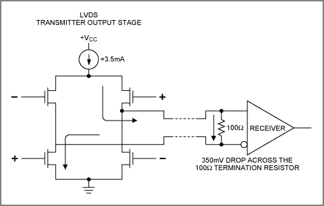
Figure 1. LVDS drivers that use a current-steering output configuration reduce ground bounce compared with voltage-mode drivers used in other differential signaling standards. LVDS drivers also eliminate shoot-through current.
In addition to the benefits discussed above, LVDS serializers and deserializers will also contribute significant space and cost savings to base-station designs. To service the bandwidth required in 3G networks new base stations will require a greater number of cards compared with 2G systems. This is especially true for baseband cards which perform the heavy digital signal processing required for spread-spectrum, interleaving, and error-control techniques. As data throughput increases between these cards, traditional TTL backplanes will no longer be sufficient. TTL cannot switch at high enough speeds, and wide parallel buses require large and expensive backplanes which increase system size and cost. The MAX9205serializer and MAX9206 deserializer solve this problem by converting 11 TTL lines (10 data + 1 clock) into just one high-speed LVDS pair (Figure 2). This approach reduces interconnect complexity by five times. In base stations with high card counts such as 3G systems, these two devices provide considerable savings in space and cost.
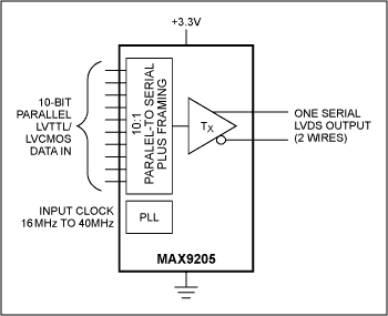
Figure 2. An LVDS serializer, used in combination with a deserializer (not shown), eliminates the wide data buses and associated large, expensive backplanes required when standard TTL signaling is used. Also, these LVDS circuits switch at the speeds required for 3G networks.
The MAX9205 serializer converts 10-bit wide, parallel LVTTL/LVCMOS data into an LVDS serial data stream. A high-state start bit and a low-state stop bit, added internally, frame the 10-bit parallel input data and ensure a transition in the serial data stream. Therefore, 12 serial bits are transmitted for each 10-bit parallel input. The MAX9205 accepts a wide 16MHz to 40MHz reference clock to produce a serial data rate from 192Mbps (12 bits x 16MHz) to 480Mbps (12 bits x 40MHz). However, since only 10 bits are from input data, the actual throughput is 10 times the reference clock frequency. The MAX9206 deserializer receives the serial output from the MAX9205 and converts it back to 10-bit-wide parallel data. Because the deserializer recovers both clock and data from the serial data stream, clock-to-data and data-to-data skew that would be present with a parallel bus is eliminated. Together, the MAX9205 and MAX9206 form a complete solution for reducing card-to-card interconnect.
The partitioning of these functions into two ICs versus a single integrated SerDes is ideal for 3G base stations, which commonly employ unidirectional links. For example, a baseband receive card might be dedicated to performing signal processing on data received from a radio transceiver card. With the approach described here, only deserialization would be required on the baseband card. Therefore, an integrated SerDes would consume extra space and add cost versus the standalone deserializer.
In base stations already employing serialized backplanes, an LVDS multiport repeater can further reduce board space and cost. Most base-station architectures contain cards that must broadcast or transmit their data to multiple destination cards. For example, many systems employ multiple baseband cards in parallel to process received data from a single radio transceiver card. The brute-force implementation of this architecture would require the radio card to include as many serializers as there are deserializers on the destination baseband cards (Figure 3a). By using a multiport repeater such as the MAX9150, this serializer count can be reduced by as much as 10:1 (Figure 3b). When used with a single serializer, the MAX9150 replaces 10 serializers with only one. This architecture is effective only with multiport repeaters specified with sufficiently low jitter. Jitter, the deviation from the ideal timing of an event or signal edge, prevents the deserializer from successfully recovering clock and data from a serial bit stream. The jitter budget for a typical LVDS serializer/deserializer pair can be as low as several hundred picoseconds. This budget is further reduced by jitter resulting from traces, cables, and connectors in the signal path. Therefore, additional devices in the signal path between a serializer and deserializer must exhibit extremely low jitter. The MAX9150 guarantees only 120ps (max) peak-to-peak jitter.
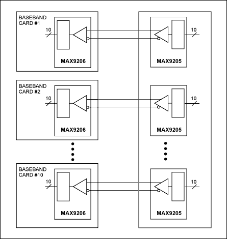
Figure 3a. When multiple baseband cards process received data from a radio transceiver card, the radio card typically includes as many serializers as there are deserializiers on the destination baseband cards.
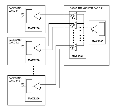
Figure 3b. By using a multiport repeater like the MAX9150, the serializer count on the radio transceiver card can be reduced by as much as 10:1
In other parts of the high-speed serial signal path, base-station architectures often require simple switching, multiplexing, and repeating functions. As in the example of the multiport repeater, these functions must be provided with minimal impact to the jitter budget. The MAX9152 2x2 LVDS crosspoint switch provides several of these functions in one package. It includes two LVDS/LVPECL inputs, two LVDS outputs, and two logic inputs that determine which inputs are connected to which outputs inside the IC. It can be programmed to connect any input to either, or both, outputs. It can be used in the following configurations: 2x2 crosspoint switch, 2:1 mux, 1:2 demux, 1:2 fanout buffer, or dual repeater. This flexibility makes the MAX9152 ideal for protection switching for fault tolerance, loopback switching for diagnostics, fanout buffering for data distribution, and signal regeneration for communication over extended distances. The MAX9152's ultra-low 120ps (max) peak-to-peak jitter ensures reliable communications in high-speed serial links.
In lower-speed signal paths, such as clock-distribution networks and control buses, LVDS is also improving performance by replacing older signaling standards like TTL and RS-422. In base-station radio transceiver cards, where there is high sensitivity to radiated noise, LVDS is the ideal signaling standard for distributing the reference clocks used by PLL frequency synthesizers. Although these circuits do not require the speed of LVDS (base-station reference clocks typically run in the tens of MHz), they benefit from LVDS's low power consumption and low radiated noise. Low-speed control buses, used for arbitration, handshaking, and other peripheral communications between cards, also benefit from the noise and power reduction from LVDS. Level translators, used solely to translate signals between LVTTL/LVCMOS and LVDS, provide a simple means of constructing LVDS clock distribution networks and control buses from existing LVTTL/LVCMOS designs. Analog's family of single, dual, and quad line drivers and receivers are the ideal building blocks for such networks, as they include some of the smallest (SC70 and SOT23 packages) and lowest pulse-skew devices available. (Pulse skew is the predominant measure of jitter in these devices.)
Summary
By exploiting the benefits of LVDS in clock distribution, control buses, backplanes, and other areas of high-speed signal distribution, 3G base stations deliver higher bandwidth wireless services without requiring proportionately greater cost, size, and power. The products discussed in this article offer these benefits not only through the LVDS signaling standard, but also from the architectures and topologies that they enable. There is no doubt today that comprehensive familiarity with LVDS technology, products, and applications is essential for any engineer developing next-generation cellular base stations.


