
Inverting Buck-Boost Compensation Cookbook
Key Takeaways
|
Abstract
This article describes a systematic method for designing a Type-II (two-pole, one-zero) voltage-mode compensator for monolithic inverting buck-boost (IBB) converters, including standard buck regulators configured for negative output operation. The article begins with power-stage design considerations for a given set of electrical requirements and derives the small-signal control-to-output transfer function for peak current-mode control. Based on this model, a practical compensator is synthesized to achieve adequate loop stability and transient response. Design equations are summarized in a step-by-step procedure, and the resulting loop characteristics are verified using LTspice® simulations. This article serves as a practical reference for voltage-loop compensation of IBB converters.
Introduction
Many electronic systems require one or more negative supply rails, typically implemented alongside corresponding positive rails to form symmetrical power supplies. These negative voltages are essential for proper biasing, signal swing, and device operation in various applications, such as:
- Gate driver circuits for power electronics in electric vehicles, enabling efficient switching of wide-bandgap devices like gallium nitride (GaN) FETs and insulated-gate bipolar transistors (IGBTs) in chargers and traction inverters.
- Precision analog front ends, including high-resolution analog-to-digital converters (ADCs), digital-to-analog converters (DACs), and rail-to-rail operational amplifiers, where negative rails allow full dynamic range and linearity in industrial and medical instrumentation.
- LCD biasing for consumer electronics, where negative voltages are required for proper pixel control and contrast adjustment.
- Photodiode biasing, including avalanche photodiodes, to achieve high-speed response and low noise in optical sensing systems.
- Medical imaging equipment, such as X-ray generators, which rely on negative voltages for detector bias and signal conditioning.
Negative rails are typically generated using an inverting buckboost (IBB) topology. In monolithic implementations, this can be realized in two common ways.
- Dedicated IBB regulator ICs.
- Standard buck regulators reconfigured for inverting operation by rerouting the power stage.
Figure 1 shows a dedicated IBB solution, while Figure 2 illustrates a buck regulator configured as an IBB.
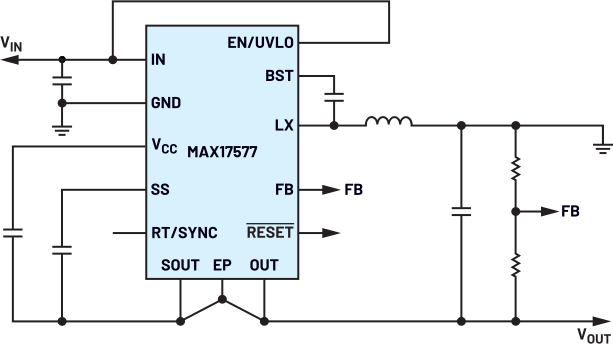
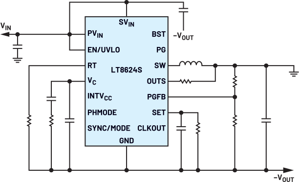
This article analyzes both approaches using a practical design example. The small-signal power-stage transfer function is derived for peak current-mode control operating in continuous conduction mode (CCM). Using this model, a voltage-loop compensator is designed to achieve a target bandwidth and phase margin. For devices with internal compensation, designers should follow the recommendations provided in the respective data sheets.
| Parameter | Value |
| Input voltage, VIN | 5V |
| Output voltage, VOUT | –5V |
| Load current, IOUT | 1A |
| Switching frequency, fSW | 3.3MHz |
| Efficiency, η | 90% |
| Upper feedback resistor, Ru | 454kΩ |
| Lower feedback resistor, Rb | 49.9kΩ |
| Load resistor, R | 5Ω |
| Power block transconductance, Gm | 6S |
| Transconductance of error amplifier, gm | 12ms |
- Continuous conduction mode (CCM)
- Peak current-mode control
- Small-signal linear operation around the steady-state operating point
- Absolute value of VOUT is used in duty-cycle and power calculations
- The analysis assumes a peak current-mode controlled converter with internal slope compensation and a high-bandwidth inner current loop, allowing the outer voltage loop to be modeled using a Type-II compensator.
Design of Power Stage
The steps for designing the power stage are as follows:
1. For an IBB converter, the ideal duty cycle is calculated using the magnitude of the output voltage:
2. The average current through the inductor is determined as:
3. The peak inductor current can be calculated using the following expression, assuming an AC ripple current of 30% of the average inductor current (represented by 0.3):
where:
4. The inductor to be selected should have an I rms rating greater than IL, and ISAT rating greater than IL,peak. The inductance required is determined as:
For buck converter ICs configured in IBB mode with a duty cycle greater than 50%, the selected inductance must exceed the minimum required inductance Lmin, as specified in the respective product data sheet. An example formula from the LT8624S is:
When applying the Lmin formula for the IBB configuration, replace VIN with VIN + |VOUT|, and use the duty cycle D, calculated in Step 1. The resultant formula is:
5. The right-half-plane (RHP) zero is determined as per the following expression:
Since Vout is negative, the absolute value of the same is considered.
6. The target crossover frequency, fcr, is at a range of 0.1 × frhp to 0.3 × frhp. Selecting fcr = 0.3 × frhp Hz.
7. Considering a step load current, ISTEP = 0.5 × IOUT for a 3% VOUT ripple (ΔVOUT = 0.03 × VOUT), the output capacitance is calculated as:
Note the COUT value calculated is derated to VOUT.
8. The slope compensation, SE, is determined from Equation 7, which is the denominator, that is 2.5 × fSW A/s.
9. The current sense resistance, Ri, can be approximated by:
Generally, the slope and the current sense information are not made directly available in the data sheet.
10. Evaluate the inductor current slope SN as:
11. The power stage output to control transfer function thus obtained is:
where:
Rc is the ESR of the output capacitor in Ω
The parameters calculated and finalized as per the design considerations are shown in Table 2.
| D | 0.5 | COUT (F) | 11.79µ |
| L (H) | 2.7µ | KVCI | 12.18 |
| frhp (Hz) | 147.365k | ωrhp (rad/s) | 925.925k |
| fcr (Hz) | 45k | ωpl (rad/s) | 31.343k |
Design of External Compensator
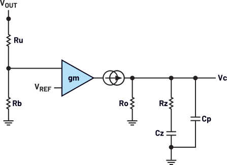
Figure 3 represents a two-pole, one-zero voltage Type-II voltage-loop compensator. The transfer function of the same is:
The combination of the control to output transfer function and the output voltage feedback provides insight into designing the compensator transfer function. The guidelines below are followed for the same:
1. The additional gain required for the loop transfer function to obtain the required bandwidth:
where:
2. The phase shift of the power stage transfer function as:
3. For a buck-boost converter, a good phase margin (PM) is above 45°. Selecting a PM of 60°, the phase boost required is:
4. The factor k is evaluated as:
5. The compensator pole ωpc and compensator zero ωzc are obtained as:
6. The integrator gain is obtained as:
7. The components for the above compensator are designed as:
Table 3 shows the compensator designed for the power stage.
| ωpc (rad/s) | 3.696M | Cp (F) | 433.954p |
| ωzc (rad/s) | 21.625k | Cz (F) | 74.184n |
| Kv (s/rad) | 161.758k | Rz (Ω) | 623.345 |
LTspice® Simulation and Observations
The simulation of the IBB stage, configured with the parameters derived in Table 3, is shown in Figure 4.
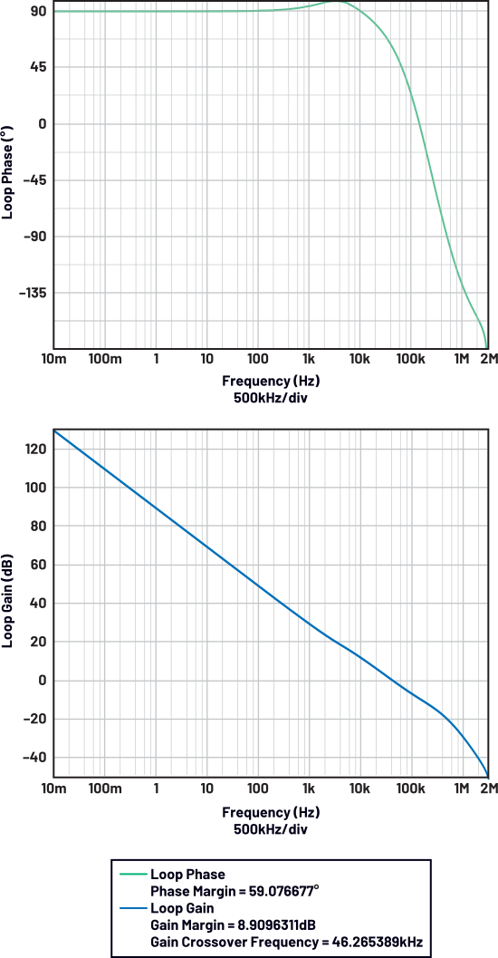
At a crossover frequency of 46.269kHz, the loop exhibits a gain margin (GM) of 8.90dB and a PM of 59.07°, GM is expected to be greater than 10dB. This can be improved by tuning the compensator pole. In this design, transient response was prioritized over gain margin, resulting in a measured GM of 8.9dB, which is acceptable for the intended operating range.
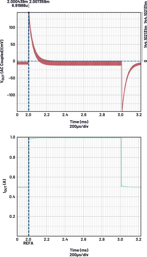
During the load step, the transient waveform exhibits an output-voltage excursion of roughly 2.88%, indicating the converter’s dynamic response characteristics.
Design Sensitivity
From the above analysis, it is evident that the selection of the inductor, L, directly influences the location of the RHP zero and, consequently, limits the maximum achievable crossover frequency of the IBB converter. The choice of output capacitance, COUT, not only determines the output-voltage excursion during load transients, but together with its equivalent series resistance (ESR) and the inductor, L, also shapes the dominant power stage pole. These parameters collectively dictate the required loop gain and phase boost during compensator design, and therefore ultimately determine the resulting phase margin of the system.
Final Design Checklist
The checklist below outlines the essential design requirements:
- High RHP zero for adequate bandwidth (via inductance selection).
- PM > 45°.
- GM ≥ 10dB is recommended; however, slightly lower GM may be acceptable when transient performance is prioritized.
- Output voltage deviation ≤ 3% during load transients.
Conclusion
This article presents a structured and repeatable approach for compensator design in IBB converters. By deriving the small-signal power stage model and explicitly accounting for the RHP zero, designers can select an appropriate loop bandwidth and compensation network. LTspice simulations confirm that the proposed method achieves stable operation and fast transient response, making it suitable for a wide range of negative-rail generation applications.
References
- Basso, Christophe P. Switch-Mode Power Supplies, Second Edition. McGraw-Hill Professional, February 2008.
- Lamp, Erik. “Fast-Transient Negative Voltage Rail for Noise-Sensitive Applications.” Analog Devices, Inc., July 2024.
- Lamp, Erik and Randyco Prasetyo. “Generating Negative Voltages from a Positive Voltage Supply: Market Requirements and Solutions.” Analog Devices, Inc., September 2024.
- Mitra, Dipankar. “How to Use the MAX17501 and MAX17502 for Negative Output Voltage Applications.” Analog Devices, Inc., April 2014.
- Nelson, Carl. “AN19—LT1070 Design Manual.” Linear Technology, June 1986.
- Ridley, Raymond B. “A New Small-Signal Model for Current-Mode Control.” Ridley Engineering, Inc., 1999.