High Speed Low Noise Op Amp Family Challenges Power and Distortion Assumptions with Rail-to-Rail Inputs and Output
High Speed Low Noise Op Amp Family Challenges Power and Distortion Assumptions with Rail-to-Rail Inputs and Output
Aug 1 2002
Introduction
The trade-off is all too familiar; low noise op amps dissipate high power. The 1.9nV/√Hz LT6202, however, doesn’t follow this rule. It provides rail-to-rail input and output operation (meaning that maximum dynamic range can now be extracted on low supply voltages) with a supply current of only 2.5mA. The LT6200 offers even lower noise (0.95nV/√Hz) and distortion, and it includes a shutdown feature for standby conditions. These unity gain stable amplifiers are well suited to fast low noise applications because of their respective 100MHz and 165MHz gain bandwidth, low distortion, guaranteed noise specifications, and low offset voltage. The amplifiers operate on a total supply voltage of 2.5V to 12.6V, and are fabricated on Linear Technology’s high speed complimentary bipolar process. All are specified with 3V, 5V, and ±5V supplies. The single LT6202, dual LT6203 and quad LT6204 are identical except in the number of op amps; likewise for the single LT6200 and dual LT6201.
Do the Math
The product of noise voltage and square root of supply current, en • √ISUPPLY, is a useful way to gauge the performance of fast low noise amplifiers. Amplifiers with low en have high √ISUPPLY, and in applications that require low noise with the lowest possible supply current, this calculation proves to be enlightening. For example, the LT6202 has an en • √ISUPPLY product of 3nV√mA/Hz, while the LT6200 en • √ISUPPLY product is only 3.9nV√mA/Hz. It is common to see similar amplifiers with much worse en • √ISUPPLY products of 4.1 to 13.2nV√mA/Hz.
An important consideration in applying the LT6200 is that noise of 0.95nV/√Hz is equivalent to the thermal noise of a 56Ω resistor. If the total source resistance exceeds this value, the source resistance dominates the noise of the circuit; not the noise of the LT6200. Figure 1 illustrates this effect by showing the total amplifier noise vs unbalanced source resistance. At low source resistance the total noise is dominated by the amplifier’s noise voltage. When source resistance is between 56Ω and approximately 1.5kΩ, the noise is dominated by the resistor thermal noise. At high source resistance the total noise is set by the product of the amplifier noise current and the source resistance.
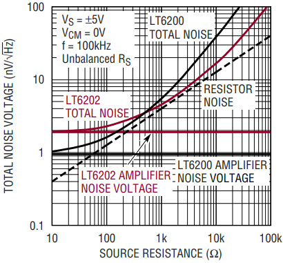
Figure 1. LT6200 and LT6202 total noise vs source resistance.
In the case of the LT6202, also shown in Figure 1, the source resistance conditions are less severe. The noise of 1.9nV/√Hz corresponds to the thermal noise of a 230Ω resistor. In the region between 230Ω and approximately 20kΩ the noise is dominated by the resistor thermal noise. Beyond this resistance the noise is set by the amplifier noise current. Below 500Ω of unbalanced source resistance, the LT6200 has lower total noise; above 500Ω, the LT6202 has lower total noise.
Low Noise and Low Distortion Design
An important rule of low noise bipolar amplifier design is that transistor noise voltage is proportional to the square root of the intrinsic base resistance rb, and inversely proportional to the square root of the transistor operating current. This means that for low noise voltage the input transistors need to be physically large to reduce the rb, and need to operate at high collector currents. In other words, halving the noise of the LT6202 requires input transistors four times larger operating at a minimum of four times the quiescent current, and this is exactly how the ultra low noise LT6200 was created. Additional current in the output stage is required to reduce the LT6200 distortion, shown in Figure 2, to an impressive –85dBc HD2, and –95dBc HD3 at 1MHz with RL = 100Ω.
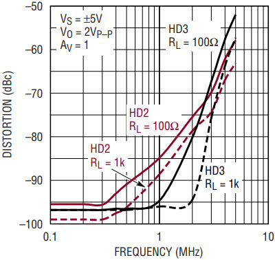
Figure 2. LT6200 distortion vs frequency
To see how these principles are applied, Figure 3 shows two parallel input stages of the op amps. This topology accomplishes several difficult tasks. First, PNP and NPN transistors in parallel reduce the effective rb by a factor of 2 and the noise voltage by the √2. Second, the input stage can common mode from the positive supply to the negative supply. The trade off between low noise design and rail-to-rail input operation is evident in that higher collector current in Q1, Q2, Q3 and Q4 means lower noise voltage, but it also means a larger voltage drop across the collector loads R1, R2, R3 and R4, and less common mode range due to saturation of the input transistors. The input referred noise benefits further from high current in the second stage Q5, Q6, Q7 and Q8, but unfortunately this current further reduces the common mode range of the input stage. The saturation of the input transistors places an upper limit on operating currents and therefore amplifier noise.
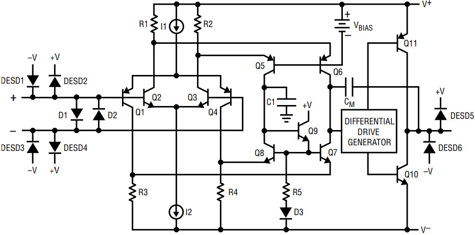
Figure 3. LT6200-4 simplified schematic
When the common mode voltage is in the middle of its range, the input stage transconductance is set by both input pairs. As the common mode voltage approaches either supply, the positive rail for instance, I1 saturates and Q1 and Q4 cutoff. At this point the input gm is reduced by half and is now set by Q2 and Q3 operating currents. With half the input stage gm, the LT6202 offset voltage shifts by about 500µV, the gain bandwidth drops to 50MHz, and the noise voltage has the spectrum shown in Figure 4.The inputs can common mode to either rail, but as a practical matter for measuring noise the inputs must be taken a few hundred millivolts from the rails. The PNP stage alone has lower noise than the NPN stage alone, and this is attributed to lower rb of the PNP transistors.
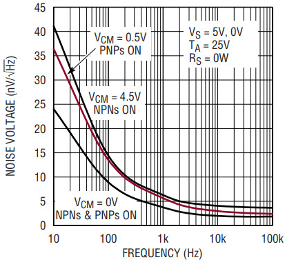
Figure 4. LT6202 noise voltage vs frequency
What about the ACs?
Capacitor C1 is used to reduce the input gm versus frequency to avoid excess phase shift through the current mirror Q7 and Q8. This capacitor provides a single high frequency path to the collectors of Q6 and Q7. The compensation capacitor CM produces a single pole open loop response, and lowers the AC output impedance.
There is a trade-off between noise and slew rate in high speed amplifiers. The commonly used technique to obtain high slew rates is to reduce the input stage gm by using input degeneration resistors, allowing for a proportional reduction in the compensation capacitor. Although this technique maintains the same gain bandwidth and yields a direct improvement in slew rate, it also causes a large degradation in the noise performance. For this reason, this family uses no input gm reduction, favoring low noise over high slew rate. The slew rate and gain bandwidth could also have been increased by reducing the compensation capacitor, resulting in the amplifier being stable only at closed loop gains >1. One reason, however, for making the amplifiers unity gain stable is to allow the closed loop gain to be rolled off with a feedback capacitor to further reduce the noise by limiting the bandwidth.
The LT6202 can drive capacitive loads as high as 100pF, while the faster LT6200 can drive 30pF. Table 1 shows a performance summary for both families.
| LT6200/LT6201 |
LT6202/LT6203/LT6204 |
||||||||
| Parameter | Conditions |
Min | Typ | Max | Min | Typ | Max | Units | |
| Offset Voltage |
VCM = VS/2 |
100 | 1000 | 100 | 500 | µV | |||
| VCM = V+ to V– |
0.6 | 2.0 | 0.8 | 2.0 | mV | ||||
| Input Bias Current | 10 | 40 | 1.3 | 7.0 | µA | ||||
| Noise Voltage |
f = 10kHz, VS = ±5V |
1.4 | 2.3 | 2.8 | 4.5 | nV/√Hz | |||
| f = 100kHz, VS = ±5V |
0.95 | 1.9 | nV/√Hz | ||||||
| Noise Current |
f = 10kHz |
Balanced RS | 2.2 | 0.75 | pA/√Hz | ||||
| Unbalanced RS | 3.5 | 1.1 | pA/√Hz | ||||||
| Large Signal Gain |
VO = 0.5V to 4.5V, RL =1k to VS/2 |
40 | 70 | 70 | 120 | V/mV | |||
| VO = 1V to 4V, RL = 100Ω to VS/2 |
11 | 18 | 8 | 14 | V/mV | ||||
| Common Mode Rejection Ratio | VCM = V+ to V– |
65 | 90 | 60 | 83 | dB | |||
| VOUT Low | ISINK = 20mA |
150 | 290 | 240 | 460 | mV | |||
| VOUT High | ISOURCE = 20mA |
220 | 400 | 325 | 600 | mV | |||
| Supply Current | Per Amplifier |
16.5 | 19 | 2.5 | 3 | mA | |||
| Disabled Supply Current | VSHDN = 0.3V |
1.3 | 1.8 | NA | mA | ||||
| Gain Bandwidth Product | VS = –5V, f = 1MHz |
165 | 100 | MHz | |||||
| Slew Rate | AV = –1, RL= 1kΩ, VO = 4V |
35 | 50 | 17 | 35 | V/µs | |||
| Distortion |
AV = 1, 1MHz, VO = 2VP–P |
HD2, RL= 100Ω | –85 | dBc | |||||
| HD3, RL= 100Ω | –95 | dBc | |||||||
| HD2, RL= 1k | –81 | dBc | |||||||
| HD3, RL= 1k | –81 | dBc | |||||||
Applications
Low Noise 4-Wire to 2-Wire Local Echo Cancellation Differential Receiver
Figure 5 shows a low noise 4-wire to 2-wire local echo cancellation differential receiver. With the LT1739 drivers in shutdown, the resulting noise is that of the LT6203 alone. The total integrated noise of the differential receiver is shown in Figure 6 from 25kHz to 150kHz.
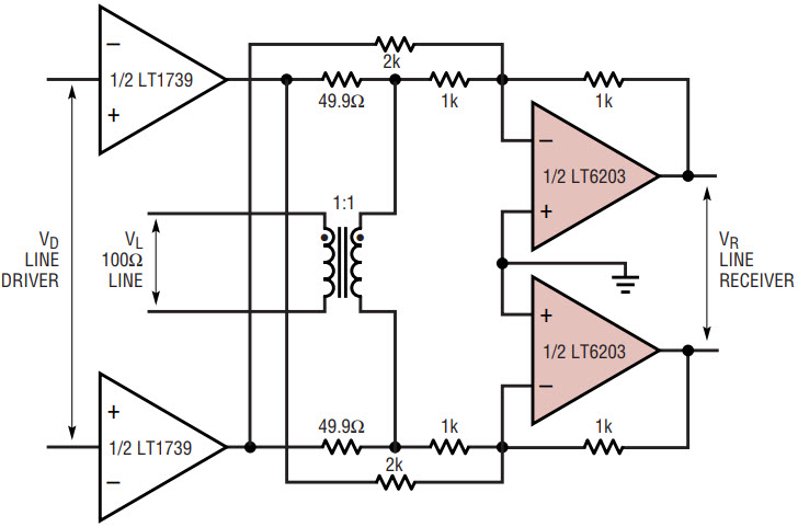
Figure 5. Low noise 4- to 2-wire local echo cancellation differential recieiver
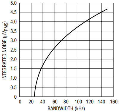
Figure 6. Line receiver integrated noise 25kHz to 150kHz
Single Supply, 1.5nV/√Hz
, Photodiode Amplifier
Figure 7 shows a simple, fast, low noise photodiode amplifier. Feedback forces the BF862 JFET source to 2.5V, which causes the drain current to be 2.5mA. At this current, the VGS of the JFET is about –0.5V, so the gate and output voltage both sit at about 2V DC and the photodiode sees 2V of reverse bias. Under illumination, the gate stays at constant DC voltage while the op amp output rises by IPD • RF, giving the transfer function VOUT = 2V + IPD • RF.
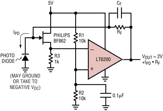
Figure 7. Single supply, 1.5nV/√Hz, photodiode amplifier
Amplifier input noise density and gain-bandwidth product were measured to be 1.5nV/√Hz and 157MHz, respectively, while consuming only 100mW. The reason the 165MHz gain bandwidth product of the LT6200 is not severely compromised by this composite circuit is that the JFET has a high gm, approximately 1/50Ω, and looks into 1kΩ so loop attenuation is only 5%. Total circuit input capacitance including board parasitics was measured to be 3.2pF. This is less than the specified CGS of the JFET, because the JFET source is not grounded but rather looks into R3 and the high impedance op amp input. This fact combined with the low input voltage noise makes the circuit well suited to both large and small photodetectors. The unity-gain stability and ultralow bias current of the circuit means that the transimpedance gain, set by RF, can be any value from 10Ω to 10GΩ.
The circuit was tested using a small 2.5pF Advanced Photonix avalanche photodiode #012-70-62-541 reverse biased to –180V, and a 210kΩ feedback resistor RF. This photodiode was selected for its speed, so that its inherent response would not impact the circuit bandwidth measurement. With feedback capacitance adjusted for 4% overshoot, closed loop bandwidth was measured to be 4.5MHz. This is in good agreement with theory given the ~5.7pF total input C and the 210kΩ transimpedance gain: 5.7pF is 6.2kΩ at 4.5MHz, for a noise gain of 210k/6.2k = 35, and a GBW product of 35 • 4.5MHz = 157MHz.
Conclusion
Linear Technology’s new family of low noise op amps operate rail-to-rail input and output while maintaining a light appetite for supply current. This combination is accomplished without sacrificing AC or DC performance. The family is available in singles, duals and quads and in a wide variety of packages.
About the Authors
Glen Brisebois is an applications engineer with the Signal Conditioning Group at Analog Devices in Silicon Valley. He attended the University of Alberta in Canada, achieving bachelor’s degrees in both physics and electrica...
