How to Design an Isolated, High Frequency, Push-Pull DC/DC Converter
How to Design an Isolated, High Frequency, Push-Pull DC/DC Converter
by
Dawson Huang
Apr 1 2015
A simple push-pull DC/DC converter with a fixed 50% duty cycle is often used as a low noise transformer driver in communication systems, medical instruments and distributed power supplies. This simple scheme provides no voltage regulation—requiring a low dropout (LDO) post regulator—a combination that presents potentially serious problems. First, any significant variation in the driver’s input voltage, along with the fixed 50% duty cycle, can increase the differential voltage across the LDO, resulting in significant power losses and high temperature rise in the LDO. Second, low switching frequency requires relatively bulky transformers, sometimes occupying 30% to 50% of the converter space.
The LT3999 monolithic DC/DC push-pull driver avoids these issues with two important features: duty cycle control and high frequency operation:
- Duty cycle control allows compensation for wide VIN variation—something standard fixed duty cycle transformer drivers cannot do—greatly reducing LDO loss when facing a wide input range.
- High switching frequency, up to 1MHz, leads to smaller transformers and lower output ripple.
The LT3999 combines these two features with high 36V input voltage and 1A input current capabilities, making it a high power and flexible low noise push-pull converter IC.
This article presents two step-by-step design procedures: One for a push-pull DC/DC converter with a wide input range, the other for a compact high frequency transformer driver with fixed input voltage.
Push-Pull DC/DC Converter Design For Wide Ranging Input
The flowchart in Figure 1b shows how a push-pull converter can be designed in eight simple steps. These steps produce the LT3999 10V–15V input, ±12V output, 200mA 1MHz push-pull converter shown in Figure 1a.


Step 1: Set the Switching Frequency (RT)
First, set the switching frequency with RT; the value chosen from Table 1 in the LT3999 data sheet.
RT = 12.1k sets fSW = 1MHz.
Step 2: Set the Input Voltage Range (UVLO, OVLO/DC)
The UVLO (undervoltage lockout) and OVLO/DC (overvoltage lockout/ duty cycle) pins are used to set input voltage range. Either a 2- or 3-resistor method can be used. For the 2-resistor method shown in Figure 2a, RB is calculated using equations 1 and 2 for UVLO and OVLO/DC, respectively. For low loss, we can assume RA = 1MΩ.

For the 3-resistor method shown in Figure 2b, RA1 and RB are calculated by equations 3 and 4 for UVLO and OVLO/DC, respectively. RA2 can be chosen around 1MΩ.

For the 2-resistor method used in Figure 1a:
VIN(MIN) = 10V, RA = 1M, RB = 143k.
VIN(MAX) = 15.5V, RA = 1M, RB = 86.6k.
Step 3: Set the Maximum Duty Cycle (RDC(MAX))
The maximum duty cycle (DCMAX) is determined by the switching period (TS = 1/fSW) and non-overlap time (TD(MIN)) between the two power switches, as shown in equation 5. For the 2-resistor method, RDC is calculated by equation 6. For the 3-resistor method, substitute RA = RA1 + RA2 in equation 6.
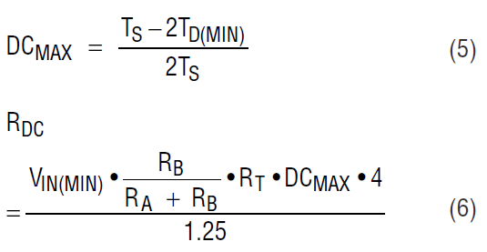
In the Figure 1(a) example, TS = 1µs, TD(MIN) = 70ns (typical value in the data sheet), VIN(MIN) = 10V, RA = 1M, RB = 143k. Calculations 5 and 6 give DCMAX = 0.43, and RDC = 13.3k.
Step 4: Select the Transformer (T1)
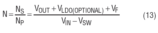
The transformer turns ratio is represented in equation 7.

VSW is the switch saturation voltage for internal switches. VF is the forward voltage of the rectifier diodes. VLDO1 and VLDO2 are the dropout voltages of the positive and negative LDOs. VSW = 0.4V, VF = 0.7V, VLDO1 = VLDO2 = 0.8V are good rules of thumb. If a commercial transformer with an exact calculated turns ratio cannot be found, select one that is close and calculate DCMAX in equation 7 accordingly. Then, recalculate RDC in equation 6 based on new DCMAX.
In the Figure 1(a) example, VOUT1 = −VOUT2 = 12V and VIN(MIN) = 10V, so choose Wurth 750314781 (N = 2) for DCMAX = 0.43.
Step 5: Design the Rectifier (D1, D2, D3 and D4)
The peak voltage across the rectifier bridge is composed of the transformer secondary side voltage (VSEC) plus any ringing voltage spikes. VSEC is calculated using equation 8. The ringing voltage spike, however, is difficult to predict, as it depends on the loop resistance, the leakage inductance of the transformer, and the junction capacitance of the rectifiers. As general rule, the rectifier voltage rating (VREC) should be at least 1.5 times the transformer turns ratio multiplied by the maximum input voltage. Because the two secondary windings are connected across the rectifier bridge, a factor of two is required, producing the formula for the rectifier voltage rating:

The current rating of the rectifier (IREC) should be greater than the load current.
When VIN(MAX) = 15.5V, N = 2, VREC ≥ 93V, IREC ≥ 200mA: a Central CMSH1-200HE (200V, 1A) satisfies these requirements.


Step 6: Select the Inductors (L1, L2)
The minimum inductor value (LMIN) is set by the peak current limit of internal switcher (ILIM) as shown by equation 9.

Higher inductance produces better regulation and lower voltage ripple, but requires a correspondingly greater volume part. The optimum inductor value is determined by taking into account both output noise and solution volume requirements.
When VIN(MAX) = 15.5V, DCMIN = 0.28, TS = 1µs, N = 2, ILIM = 1A, IOUT1 = IOUT2 = 200mA, LMIN = 38.3µH: A Coilcraft XFL3012-393MEC (39.3µH) satisfies these requirements without adding unnecessary size.
Step 7: Select the Low Dropout Linear Regulator (U2, U3)
The maximum voltage of LDO occurs at maximum input voltage under no load, when VSEC equals VIN(MAX) • N. The current rating of the LDO should be greater than the load current.
When VIN(MAX) = 15.5V, N = 2, the voltage rating for the LDOs should be 31V and −31V, satisfied by the LT3065 (45V, 500mA) and LT3090 (−36V, 400mA), respectively.
Step 8: Add a Snubber (CS and RS)
The recommended approach for designing an RC snubber (CS and RS in Figure 1) is to measure the period of the ringing at the LT3999’s SWA and SWB pins when its switchers turn off without the snubber, and then add capacitance—starting with something in the range of 100pF—until the ringing period lengthens by 1.5x to 2x.
The change in period determines the value of the parasitic capacitance (CPAR), from which the parasitic inductance (LPAR) can be determined from the initial period. Similarly, initial values can be estimated using data sheet values for switch capacitance and transformer leakage inductance.
Once the value of the drain node capacitance and inductance are known, a series resistor can be added to the snubber capacitance to dissipate power and critically dampen the ringing. The equation for deriving the optimal series resistance using the observed periods (tPERIOD, and tPERIOD (SNUBBED)) and snubber capacitance (CS) is below. Refer to the LT3748 data sheet for more details.

Results
The measured results in Figures 3, 4 and 5 show that duty cycle control in the push-pull converter of Figure 1 maintains a low VIN − VOUT differential across the LDOs, resulting in minimized power loss and temperature rise. Figure 3 shows that at 200mA per LDO, VDIFF , remains under 2.5V over the entire input voltage range of 10V – 15V. Figure 4 shows power loss remains low across the load current range. Figure 5 and Figure 6 show the thermal results.
For comparison, Figure 7 shows the efficiency comparison of the design with duty cycle control disabled and duty cycle control enabled. The efficiency drops dramatically when input voltage increases. Figure 8 shows the differential voltage across the positive LDO with duty cycle control disabled and duty cycle control enabled. Figures 9 and 10 show the thermal results. It is evident that the duty cycle control reduces the differential voltage and improves the efficiency and thermal performance.


Compact Transformer Driver For A Fixed Input Voltage
Normally, the output voltage of the basic unregulated transformer driver converter changes significantly with changes in load current. To produce a regulated voltage, an LDO on the output is strongly recommended. Figure 6a shows the schematic of low part count transformer driver using the LT3999. Figure 6b shows the design flowchart.
The four simple steps in the flowchart can be used to design a 1MHz, low parts count, 5V input, 5V output 400mA output transformer driver as an example.
Step 1: Set the Switching Frequency (RT)
The switching frequency of the LT3999 is set by a single RT resistor selected based on the table in the LT3999 data sheet (frequency range is from 50kHz to 1MHz).
In the design example, for high frequency fSW = 1MHz, RT = 12.1k.
Step 2: Select the Transformer (T1)
The transformer turns ratio is determined by:
where VSW is the switch saturation voltage for internal switchers, and VF is the forward voltage of a rectifier diode.


VLDO is the drop from the unregulated transformer driver output to the post regulated low noise output. VLDO is the drop at highest current, so it should be minimized. 0.8V provides enough drop to avoid dropout without the LDO getting hot. A good rule of thumb assumption is VSW = 0.4V, VF = 0.7V, VLDO = 0.8V.
The current rating of the transformer should be 20%~50% larger than the output current to leave some room.
The sum of the peak magnetizing current (IM(PEAK)) and the full load current reflected to the primary side (N • IOUT) should less than the peak current limit of the internal switcher (ILIM). Based on this, minimal LM (LM(MIN)) is required.


IM(PEAK) + N • IOUT

For VOUT = VIN = 5V, the Coilcraft P
Step 3: Rectifier (D1, D2)
Choose the rectifier diodes based on voltage and current. The voltage across the diodes is more than twice that of the transformer secondary voltage because of its center tap structure. The voltage rating of the rectifier should be larger than 2N • VIN = 15V, maybe by 20%.
The CMSH1-20M (20V, 1A) satisfies these requirements.


Step 4: Low Dropout Linear Regulator (U2, Optional)
The maximum input voltage of the optional post-regulating LDO (VLDO_IN(MAX)) occurs at no load, where it equals VIN • N = 7.5V. The current rating of the LDO should be larger than the load current (>400mA in the case of the design example).
A good LDO for the 5V, 400mA output is the LT1763 (20V, 500mA).
Conclusion
The LT3999 is a monolithic DC/DC transformer driver, which features duty cycle control, high frequency and high power. It allows a wide input voltage range and low loss at the LDO, while using small passive components due to its high frequency operation. It also features input voltage up to 36V and input current up to 1A.
About the Authors
Dawson Huang joined Linear Technology Corporation in 2014 as an applications engineer. His work includes development, evaluation and characterization of new power management ICs. He is also in charge of circuit design and
Related to this Article
Products
RECOMMENDED FOR NEW DESIGNS
45V VIN, 500mA Low Noise, Linear Regulator with Programmable Current Limit and Power Good
RECOMMENDED FOR NEW DESIGNS
500mA, Low Noise, LDO Micropower Regulators
PRODUCTION
Low Noise, 1A, 1MHz Push-Pull DC/DC Driver with Duty Cycle Control
Product Categories


