Evaluating Power Supplies with Different Compensation Settings

Evaluating Power Supplies with Different Compensation Settings
Jul 17 2026
Key Takeaways
|
Abstract
This article explains why power supplies have regulation loops and how to optimize them to achieve the best possible performance. The performance must be tested in the lab to ensure that the design process really was accurate. Such work in the lab takes a lot of time since tweaking compensation components involves soldering of different value capacitors and resistors. By using a software-controlled compensation probe card, this soldering work is replaced by mouse clicks, saving effort and shortening evaluation time.
Introduction
Power supplies are usually intended to generate a fixed output voltage. This must not oscillate and should remain constant with load transients and changes in the input voltage. To optimize the control loop of a switch-mode power supply, compensation pins are present in many power supply ICs. These can be wired with appropriate compensation components, capacitances, and resistors to optimize the control loop to achieve the highest control bandwidth while ensuring loop stability. The reason for the adjustability of a control loop is that the compensation must be carried out differently depending on the operating conditions and the selection of external components in the power path. Figure 1 shows a buck, step-down regulator with a corresponding compensation pin, VC.
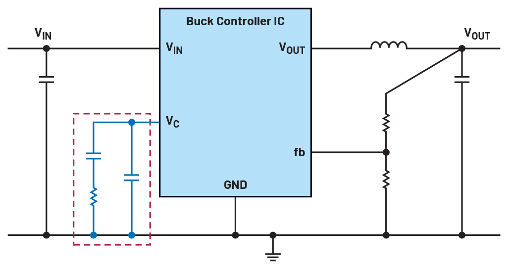
The selection of compensation components can be made with appropriate calculation and simulation programs such as LTpowerCAD® and LTspice® . However, the parasitic effects of the circuit board layout also play a certain role. Thus, a power supply should always be checked in hardware. Here, the selection of compensation components is finally checked and confirmed.
In the design process of a power supply, this step is time-consuming. A Bode diagram or a load transient measurement must be carried out with an LTpowerAnalyzer, for example. If the result obtained does not meet the design goals, it must be optimized. To do this, the compensation components are soldered out, and other values of these components are soldered in. This is a laborious and time-consuming process.
Figure 2 shows a board available from Analog Devices, which is called a compensation probe. This card can be connected to the compensation pin and to the ground pin of any power supply with the solder contacts on the right side. The board replaces the compensation components in the red rectangle in Figure 1. On the left side, the board is connected to a PC with a USB cable. After connecting the hardware, the free software for the LTpowerAnalyzer is started. In it, a graphical user interface switches between different values of the compensation components in the shortest possible time. Combined with an LTpowerAnalyzer, Bode diagrams can then be created and load transient tests can also be executed at different compensation settings.
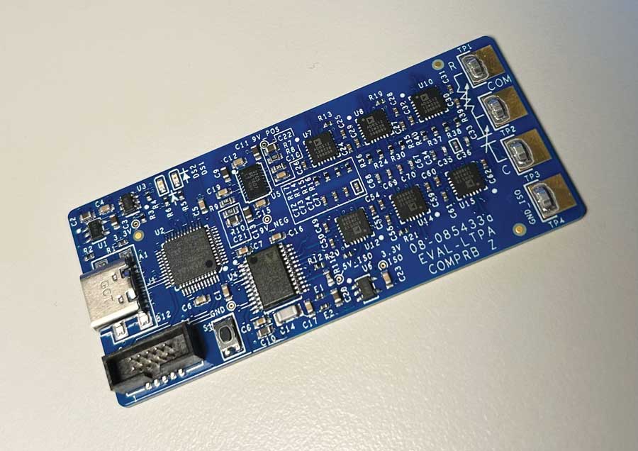
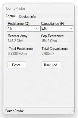
Figure 3 shows the software interface of the EVAL-LTPA-COMPRB (compensation probe) board. Here you can select settings of resistance values between 511Ω and 100kΩ and capacitor values between 5pF and 39nF. The internal series resistance of the capacitor is also displayed and considered. If this compensation board is connected to the ground connection of the power converter IC to be tested, as well as to the compensation pin, with only short connecting leads, different compensation component values can be selected precisely, easily, and quickly.
Conclusion
Checking and optimizing the control loop stability of a power supply is not only easy but also very efficient with a compensation probe, such as the EVAL-LTPA-COMPRB. Different compensation settings can be tested in no time. This not only creates better power supplies but also allows for design in less time.
About the Authors
Frederik Dostal is a power management expert with more than 20 years of experience in this industry. After his studies of microelectronics at the University of Erlangen, Germany, he joined National Semiconductor in 2001,
Related to this Article
Products
LTpowerAnalyzer Compensation Probe
EVAL-LTPA-KIT | Low-cost, High Performance, Compact Laboratory Tool for Evaluating and Characterizing Power Su...