Decrease Li-Ion Battery Charge Time with a Monolithic Charger that Prevents Overheating
Decrease Li-Ion Battery Charge Time with a Monolithic Charger that Prevents Overheating
by
Phil Juang
Mar 1 2003
Introduction
The LTC4054 is a constant-current/constant-voltage linear battery charger with an internal power MOSFET in a tiny ThinSOT package. Most linear chargers risk temporary, excessive power dissipation and possible overheating, but the LTC4054 uses internal thermal feedback to regulate the charge current and limit the die temperature to 120°C. This feature allows the designer to program the LTC4054 to higher charge currents with the assurance that the LTC4054 will not overheat and damage itself or other components. This article shows how to use the LTC4054 to maximize the thermally regulated charge current to reduce battery charging times.
The LTC4054 includes other desirable features that save space and reduce circuit costs. It does not require an external sense resistor or blocking diode because of its internal MOSFET architecture. The automatic charge termination feature allows the LTC4054 to act as a standalone Li-Ion battery charger. A charge status output pin indicates the state of the battery charger. It also includes undervoltage lockout protection, low-battery charge conditioning, a charge current monitor pin, and automatic recharge. Furthermore, the LTC4054 is capable of operating from a USB power supply.
Thermal Considerations
The thermal feedback loop of the LTC4054 regulates the die temperature to approximately 120°C by automatically reducing the charge current as the IC heats up. It follows that to maintain high charge currents (and correspondingly shorter charge times), heat must be efficiently transferred away from the LTC4054. The key quantity is the thermal resistance from the die to the PC board to ambient air (see "Thermal Resistance Calculation" below).
The thermal resistance of the LTC4054 package is dependent on board layout. Since the majority of the heat generated by the IC flows through the copper lead frame and out the package leads (especially the ground lead), the board designer can use the PCB copper as a heat sink to improve the thermal characteristics. By soldering the leads (particularly the ground lead) to wide copper pads that expand out to larger copper areas, the heat from the IC will more easily dissipate to the surrounding ambient. Feedthrough vias to inner or backside copper ground planes further improve the thermal resistance. Other sources of heat dissipation on the board should be considered during PCB layout, because they can increase the ambient temperature (TA) and reduce the maximum charge current.
Thermal Resistance Calculation
The following example calculates the maximum thermal resistance (θJA) allowed to charge a battery at 800mA assuming typical charge conditions. The thermal resistance is defined as the steady state difference in temperature between ambient and the silicon junction given a certain amount of power dissipation in the silicon. Since the majority of the power dissipation on the die comes from the internal MOSFET, the power is calculated to be:

where IBAT is the charging current, VCC is the VCC pin voltage, and VBAT is the BAT pin voltage. In this example, we will assume a nominal battery voltage of 3.7V, a 5V typical operating voltage, and an ambient temperature of 25°C.
The silicon junction temperature is calculated by the following formula:

TJ is the junction temperature and TA is the ambient temperature. The LTC4054 charges at the programmed charge current as long as the power dissipation does not generate enough heat to raise the junction temperature above its thermal regulation point of 120°C:


Assuming typical charge conditions, charging at 800mA requires a thermal resistance of less than 91°C/W. If the thermal resistance is too great, the LTC4054 automatically reduces the charge current (IBAT) to maintain a constant die temperature of 120°C.
800mA Charger Circuit
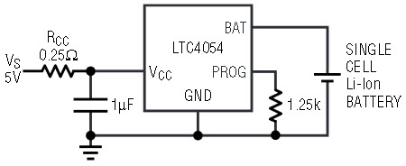
Another method of maximizing charge current is to dissipate some of the power in an external component, thus reducing the power dissipation on the die. Figure 1 shows how the LTC4054 can provide a complete standalone lithium-ion charger solution using few external components.

Figure 1. Standalone 800mA Li-Ion battery charger with external power dissipation.
The external resistor Rcc is used to dissipate 160mW of the charger’s total power dissipation, enabling the LTC4054 to thermally regulate at higher charge currents. Because the power is dissipated in an external component that also uses the PC board as its heat sink, the temperature of the die is reduced.
When this circuit is programmed to charge at 800mA, the voltage on the VCC pin drops to 4.8V. With a nominal battery voltage of 3.7V and an ambient temperature of 25°C, the LTC4054 enters thermal regulation when (see see "Thermal Resistance Calculation" in this article):

The thermal resistance of the LTC4054 can now be as high as 108°C/W before thermal regulation limits the charge current.
Dissipating power in an external component is a useful technique, especially when a high input supply voltage is used. However, the designer should avoid dropping the VCC pin voltage low enough to put the LTC4054 into dropout, which could increase the time spent charging in constant-voltage mode. This occurs when the voltage across the internal MOSFET drops low enough to cause the FET to enter the linear region. The transistor does not enter the linear region as long as the following condition is met:

The RDS(ON) of the LTC4054 FET is nominally 600mΩ. Since Li-Ion battery voltages do not typically exceed 4.2V, an LTC4054 programmed with 800mA will not enter dropout as long as the VCC pin stays above 4.68V.
Conclusion
The LTC4054 standalone Li-Ion battery charger provides a simple, compact solution for charging single cell Li-Ion batteries using very few external components. Its thermal regulation feature allows the designer to eliminate the need for thermal over-design, maximize charge current, and shorten charge times.


