AN143 - A Simple Method to Accurately Predict PLL Reference Spur Levels Due to Leakage Current
AN143 - A Simple Method to Accurately Predict PLL Reference Spur Levels Due to Leakage Current
Jan 3 2014
Presented is a simple model that can be used to accurately predict the level of reference spurs due to charge pump and/or op amp leakage current in a PLL system. Knowing how to predict these levels helps pick loop parameters wisely during the early stages of a PLL system design.
Quick Review of PLLs
The phase locked loop (PLL) is a negative feedback system that locks the phase and frequency of a higher frequency device (usually a voltage controlled oscillator, VCO) whose phase and frequency are not very stable over temperature and time to a more stable and lower frequency device (usually a temperature compensated or oven controlled crystal oscillator, TCXO or OCXO). As a black box, the PLL can be viewed as a frequency multiplier.
A PLL is employed when there is the need for a high frequency local oscillator (LO) source. Example applications are numerous and include wireless communications, medical devices and instrumentation.
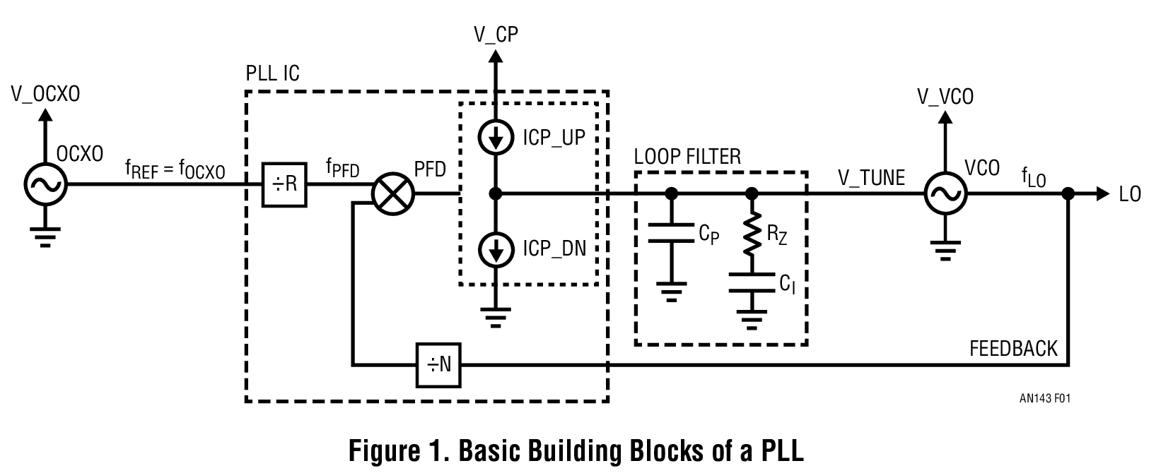
Figure 1 shows the building blocks of a PLL system used for generating an LO signal. The PLL integrated circuit (IC) usually contains all clock dividers (R and N), phase/ frequency detector (PFD) and the charge pump, represented by the two current sources, ICP_UP and ICP_DN.
The VCO output is compared to the reference clock (the OCXO output here) after both signals are divided down in frequency by their respective integer dividers (N and R, respectively). The PFD block controls the charge pump to sink or source current pulses at the fPFD rate into the loop filter to adjust the voltage on the tuning port of the VCO (V_TUNE) until the outputs of the clock dividers are equal in frequency and are in phase. When these are equal, it is said that the PLL is locked. The LO frequency is related to the reference frequency, fREF, by the following equation:
fLO = N/R * fREF
The PLL shown in Figure 1 is called an integer-N PLL because the feedback divider (the N-divider) can only assume integer values. When this divider can assume both integer and noninteger values, the loop is called a fractional-N PLL. The focus here will be only on integer-N PLLs, as different mechanisms are at work in fractional-N PLLs.

Integer-N PLL Nonidealities
The PLL IC contributes its own nonidealities to the system, principally phase noise and spurious.
Phase Noise
The PLL system of Figure 1 acts as a low pass filter on the reference clock phase noise and as a high pass filter on that of the VCO. The low pass and high pass filter cutoff frequency is defined by the loop bandwidth (LBW) of the PLL. Ideally, the LO phase noise follows that of the reference clock converted to the LO frequency (that is, multiplied by N/R) up to the LBW and subsequently follows the phase noise of the VCO. The PLL IC’s noise contribution elevates the phase noise in the transition area.
Figure 2 is a phase noise plot generated by PLLWizard, a free PLL design and simulation tool from Linear Technology. The figure shows both the total output phase noise (TOTAL), and the individual noises at the output due to the reference (REF at RF) and the VCO (VCO at RF). The IC’s noise contribution can easily be seen in the highlighted area.

Spurious
Any unwanted signals on the power supplies shown in Figure 1 (V_OCXO, V_CP and V_VCO) can translate into spurious (spurs) on the LO signal. Careful design of these supplies greatly reduces or even eliminates these spurs. Charge pump related spurs, however, are inevitable. But, they can be reduced with careful PLL system design. These spurs are commonly referred to as reference spurs, though reference here does not mean the reference clock frequency. Rather, it refers to fPFD. An LO signal produced by an integer-N PLL has dual sideband spurs at fPFD and its harmonics.
For example, Figure 3 shows the spectrum of a 2.1GHz LO signal. fPFD is 1MHz (N = 2100) and the reference clock is 10MHz (R = 10). The loop bandwidth is 40kHz. As a side note, it is worth mentioning that the spurious level achieved in this measurement is world class due to the high performance of the LTC6945, an ultralow noise and spurious PLL IC from Linear Technology.

Causes of Reference Spurs
In steady-state operation, the PLL is locked, and, theoretically, there is no more need to engage the ICP_UP and ICP_DN current sources of Figure 1 during every PFD cycle. However, doing so would create a dead zone in the loop response as there is a significant drop in the smallsignal loop gain (practically, an open loop). This dead zone is eliminated by forcing ICP_UP and ICP_DN to produce extremely narrow pulses during every PFD cycle. These are commonly referred to as anti-backlash pulses. This produces energy content on the VCO tune line at fPFD and its harmonics. The negative feedback cannot counteract these pulses since these frequencies are outside the loop bandwidth of a properly designed PLL. The VCO, then, is frequency modulated (FM) by this energy content, and related spurs appear at fPFD and its harmonics, all centered around LO.
Between anti-backlash pulses, the charge pump current sources are off (tri-stated). Inherently, the charge pump has some leakage current when tri-stated. Using an op amp in an active loop filter (such as in Figure 7) introduces yet another leakage current source due to the op amp’s input bias and offset currents. The aggregate of these unwanted currents, whether sourcing or sinking, causes a drift in the voltage across the loop filter and, consequently, in the tune voltage of the VCO. The negative feedback of the loop will correct for this anomaly by introducing a unipolar current pulse from the charge pump once every PFD cycle so that the average tune line voltage produces the correct frequency out of the VCO. The pulses produce energy at fPFD, which also causes spurs to appear centered around LO and offset by fPFD and its harmonics as previously noted.
In integer-N PLLs, fPFD is often chosen to be relatively small because of the system’s frequency step size requirements. This means that the anti-backlash pulse width, especially with the present high speed IC technologies, is extremely small compared to the PFD period. As such, a large leakage current causes the total charge pump pulses to be unipolar and tends to be the dominant cause of reference spurs. This phenomenon will be examined in more depth.
About the Authors
Will Ezell currently focuses on low noise synthesizers for 5G systems. He has previously created synthesizer and other timing products at Linear Technology, and has held design positions at Dallas Semiconductor, Microtune...
Michel Azarian is a Senior Applications Engineer at Linear Technology responsible for supporting synthesizer and timing products. Michel holds a bachelor’s degree in Electrical Engineering from the American University of B...


