Overview
Design Resources
Design & Integration File
- Schematic
- Bill of Materials
- Gerber Files
- Assembly Drawings
- Allegro Layout File
Evaluation Hardware
Part Numbers with "Z" indicate RoHS Compliance. Boards checked are needed to evaluate this circuit.
- EVAL-ADICUP3029 ($60.92) Ultralow power, Cortex M3, Arduino Form Factor Development Board
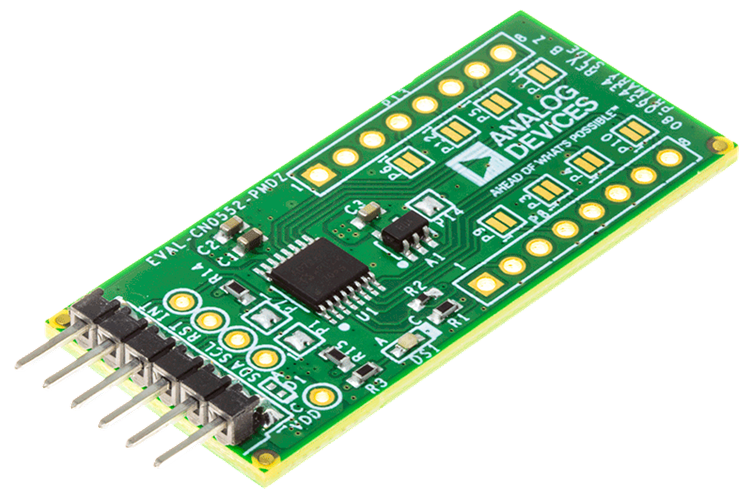
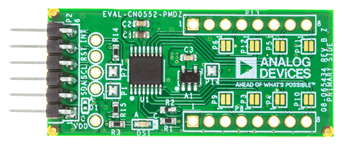
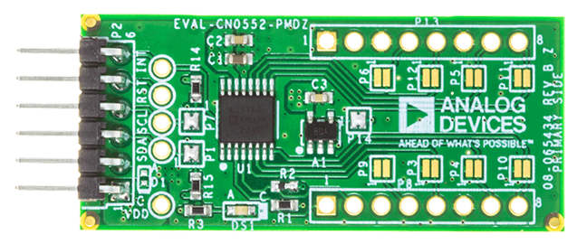
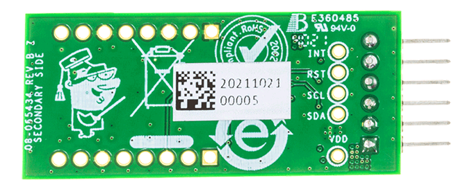
- EVAL-CN0552-PMDZ ($36.92) Extended Range Capacitance to Digital Converter
Device Drivers
Software such as C code and/or FPGA code, used to communicate with component's digital interface.
Features & Benefits
- ±4.096 pF input range suits a wide array sensors.
- Extended input range circuit provides ±50pF input range
- 4.2 aF RMS resolution @ 9.1sps conversion rate
- Auxiliary temperature sensor and voltage input for system-level calibration
Documentation & Resources
-
CN0552 User Guide11/22/2021WIKI
-
Solutions For Rapid Prototyping: Answering the Needs of Practicing Engineers8/23/2023PDF784 K
-
CN0552: Capacitance to Digital Converter with Extended Range (Rev. 0)11/19/2021PDF916 K
Circuit Function & Benefits
Capacitive sensors are used in a wide array of industrial applications such as liquid level monitoring, pressure measurement, position sensing, flowmeters, humidity sensing, and many more. ΣΔ (Sigma-Delta) Capacitance to Digital Converters (CDCs) operate by exciting the unknown capacitance with a square wave and con-verting the resulting charge into a single-bit digital output stream. A digital filter then processes the bit stream, outputting a precise, low-noise capacitance measurement.
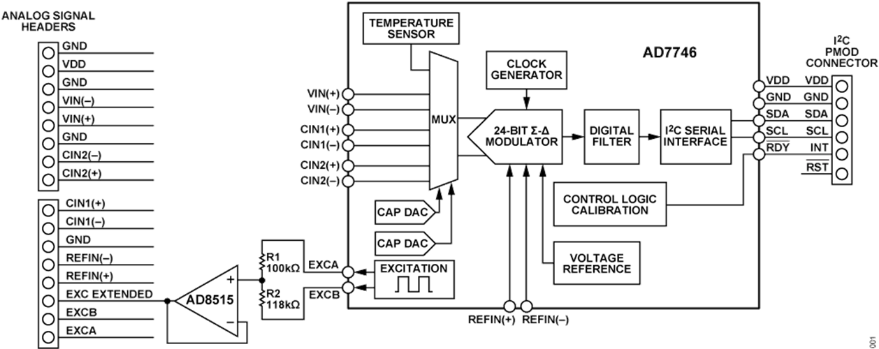
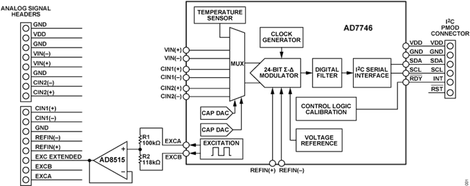
The circuit shown in Figure 1 is a 24-bit capacitance to digital converter (CDC) with a default full-scale input range of ±4.096 pF at a maximum bulk capacitance of 17 pF but is capable of extending up to ±50 pF with a maximum bulk capacitance of 200 pF. The output data rate is adjustable from 9.1 sps to 90.9 sps, with the 16.1 sps setting providing strong rejection of both 50Hz and 60Hz power line noise. The CDC also provides temperature measurement with a resolution of 0.1°C and accuracy of ±2° C for temperature compensation and system calibration.
The CN0522 is compatible with I2C Pmod platform boards, with an I/O voltage from 2.7 V to 5.5 V.

Circuit Description
Capacitance to Digital Conversion
The core of the circuit shown in Figure 1 is the AD7746, a 24-bit Σ-Δ capacitance-to-digital-converter (CDC) with an I2C serial communication interface that provides a high resolution (24-bit no missing codes, up to 21-bit effective resolution), high linearity (±0.01 %), and high accuracy (±4 fF factory calibrated) capacitance measurement. It is consists of a second-order modulator and a third-order digital filter. A square-wave excitation signal is applied to one terminal of CXn and the modulator continuously samples the resulting charge going through at the corresponding CINn pin. The modulator output is processed by the digital filter, scaled, factory calibration coefficients applied, and the final result read out through the serial interface.
The AD7746 capacitance input range is ±4.096 pF (changing). It can accept up to 17 pF common-mode capacitance (not changing), which can be balanced by a programmable on-chip, digital-to-capacitance converter (CAPDAC) and it can extend up to a ±50 pF input range (changing) using AD8515, a rail-to-rail aoperational amplifier that acts as a gain buffer that provides a drive signal to the sensor.
As shown in Figure 2, the AD7746 has two capacitive input channels, each configurable as single-ended or differential, as well as an onboard temperature sensor and an auxiliary voltage input channel. The AD7746 is designed for floating capacitive sensors. Therefore, both CX plates must be isolated from ground.

The two excitation pins EXCA and EXCB are independently programmable. They are functionally identical, therefore either of them can be used for the capacitive sensor excitation, however, it is recommended to use a separate excitation pin for each capacitive channel measurement.
CAPDAC Operation
The AD7746 includes two capacitive digital to analog converters, or CAPDACs, as shown in Figure 3. The CAPDAC can be considered as a negative capacitance connected internally to the CIN pins.
It can be used to shift the input range and compensate for the bulk capacitance of a sensor element. The CAPDAC's have 7-bit resolution and a full-scale of 21pF ± 20%. For instance, consider a sensor that has 17pF bulk capacitance. The required CAPDAC setting is calculated in the following equation:

There are two independent CAPDACs. One is connected to the CIN(+) pin and the second is connected to the CIN(-) pin but the two capacitive channels share the same CAPDACs. The relation between the capacitance inputs and the output data can be expressed as shown in Equation 1:


Capacitive Input Range
The typical capacitive measurement setup requires capacitive materials to be connected between the CIN and EXC pins of the AD7746. By default, the nominal input range is ±4.096 pF with its mid-scale value varying depending on the value set on CAPDAC. There are two measurements modes available: single-ended mode or differential mode. Using single-ended or differential as the input conversion modes will depend on the type of capacitor you are trying to measure. For example, a floating humidity sensor encased in plastic, can be treated as a single ended capacitance, as it has a very low self-capacitance which the AD7746 sees as a common-mode component. In contrast, a capacitive pressure sensor encased in a grounded stainless steel enclosure may have a common-mode capacitance that is greater than the differential capacitance. Since it is the differential capacitance that represents the sensor output, the common-mode capacitance must be at least partially canceled during the conversion process.
Single-Ended Capacitive Input
When in single-ended conversion mode, it's important to internally disconnect the CIN(-) pin on the AD7746, which is done by writing to the CAP_SETUP_REGISTER and setting the CAPDIFF bit equal to 0. Figure 4 shows the basic connection diagram for the single-ended conversion configuration.

When set up in this configuration, the CDC can measure the input capacitance in the range of ±4 pF. Table 1 shows how the CAPDAC can be used to shift the bulk capacitance input range (CX1 ) to allow for the full ± 4pF measurement span around that bulk value.
| CAPDAC(+) (pF) |
CAPDAC(-) (pF) |
CIN(+) Input Range (pF) |
Bulk Capacitance (CX) Range (pF) |
| 0 | OFF | 0 ± 4 | 0 - 4 |
| 4 | OFF | 4 ± 4 | 0 - 8 |
| 17 | OFF | 17 ± 4 | 13 - 21 |
Differential Capacitive Input
When using differential conversion mode, the AD7746 measures the difference between the CIN(+) and CIN(-) capacitance inputs. This is configured by writing the CAP_SETUP_REGISTER and setting the CAPDIFF bit equal to 1. Figure 5 shows the basic connection diagram for differential conversion.

Each of the two input capacitances CX and CY between the EXC and CIN pins must be less than 4 pF without using the CAPDACs or must be less than 21 pF and balanced by the CAPDACs. Balancing by the CAPDACs means that both CX–CAPDAC(+) and CY–CAPDAC(–) are less than 4 pF. If the unbalanced capacitance between the EXC and CIN pins is higher than 4 pF, the CDC introduces a gain error, an offset error, and a nonlinearity error. There are a few possible input ranges combinations as long as CX–CAPDAC(+) and CY–CAPDAC(–) are maintained to less than 4 pF. Table 2 shows you some of these ranges.
| CAPDAC(+) (pF) |
CAPDAC(-) (pF) |
CIN(+) Range (pF) |
CIN(-) Range (pF) |
Bulk Cap. (CX) Range (pF) |
Bulk Cap. (CY) Range (pF) |
| OFF | OFF | 0 - 4 | 0 - 4 | 0 - 4 | 0 - 4 |
| 4 | 4 | 4 ± 2 | 4 ± 2 | 2 - 6 | 2 - 6 |
| 17 | 17 | 17 ± 2 | 17 ± 2 | 15 - 19 | 15 - 19 |
Extended Input Range Circuitry
Figure 6 provides the circuitry needed for extending the capacitive input range of the AD7746 capacitance to digital converter. The extended range settings measure the capacitive value between the AD7746 CIN pins and AD8515 output. The AD8515 op amp also functions in the circuit as a low impedance source to ensure that the sensing capacitance is fully charged when the AD7746 begins sampling.

The AD7746 CDC measures capacitance using switching capacitor technology to build a charge balancing circuit, using the expression for charge, capacitance, and voltage shown in Equation 2.

Where:
Q is the charge
V is the voltage
and C is the capacitance
Therefore, the conversion result represents the ratio between the input capacitance and internal reference capacitance. The excitation voltages and the internal reference voltage have known fixed values.
The range extension circuit ensures that the charge transfer of the input capacitance remains within the input range of the AD7746. To achieve the input range extension, the excitation voltage needs to be decreased by a factor, so that the input capacitance connected to the input can be increased by that same factor. The AD7746 has two independent excitation voltage sources, EXCA and EXCB, and for the input range extension, the excitation sources have to be set up in a way that EXCB is the inverse of EXCA. The resistors (R1 and R2) shown in Figure 6 are used to calculate the resulting range extension factor using Equation 3.

Where:
F is the range extension factor
VEXC(A−B) is the voltage between the excitation sources
VEXCS is the attenuated voltage (approximately VDD/2)
and R1 and R2 are the resistor values
Range Extension Factor Calculation
To calculate the extension factor, the user must first discern which of the sensor parameters is the main contributor for the required range extension: bulk capacitance or dynamic range. Consider a typical relative humidity sensor with a bulk capacitance of 150 pF±50 pF and a slope of 0.25 pF/% RH. The bulk capacitance of the sensor can be as high as 200 pF, which results in a required range extension factor as follows:

Where:
FFIX is the range extension factor
200 pF is the maximum bulk capacitance of the sensor
17 pF is the maximum capacitance that CAPDAC can accept (in Normal Range setting)
The dynamic range of the sensor (CDYN) can be calculated from the slope of the sensor (in pF / %RH) and the full-scale input range with the following equation:

The range extension factor required for the dynamic range (FDYN) is calculated as follows:

Thus the bulk capacitance of the sensor determines the range extension factor, which should be set to 11.76.
R1 and R2 Resistor Value Selection
A value of 100 kΩ was chosen for R1. The resistor value for R2 is calculated and rounded down to the next value in the standard E96 series of resistors in the equation below which is a re-arranged formula from Equation 3 to solve for R2. Do note that a small change in the value of either resistor (R1 and R2) can significantly change the range extension factor.

Therefore,

The resistor values (100 kΩ for R1 and 118 kΩ for R2) are applied to calculate the exact range extension factor using Equation 3:

Therefore, the dynamic capacitive input range can be computed using Equation 5:

Required CAPDAC Setting
The AD7746 has CAPDACs that can be used to compensate for the bulk capacitance of a sensor element. For the AD7746, the CAPDACs have a full-scale value of 17 pF minimum and 21 pF typical. Therefore, for a given CAPDAC setting, the capacitances can vary significantly from device to device. The reason for this variance is that the AD7746 on-chip capacitances can vary with the production process from batch to batch. However, the ratio variation between the on-chip capacitances is small.
The AD7746 capacitive input is factory calibrated, and the gain calibration (GAIN_CAL) is stored in the Cap Gain Calibration register (0xF). The calibration factor stored in the Cap Gain Calibration register can be calculated using equation Equation 6:

where:
FGAIN_CAL is the gain calibration factor
GAIN_CAL is the digital code value that is stored in the Cap Gain Calibration Register (0xF)
Consider a particular device that has a factory programmed value of 0x69 (Hex) or 105 (Decimal). The gain calibration factor is:

The internal reference capacitance (CREF) can be defined as the product of the allowed full range input capacitance of the AD7746 and the gain calibration factor (FGAIN_CAL), and the value of CREF can be calculated using Equation 7:

The AD7746 is designed so that the ratio between full range CAP-DAC capacitance (CCAPDAC) and internal reference capacitance is 3.2. Therefore, the full range of the CAPDAC can be calculated using Equation 8:

For this example, CCAPDAC is:
CCAPDAC = 4.096pF × 1.002 × 3.2 = 13.13pF
The capacitance of 1LSB can be computed using Equation 9:

For this example, CLSB_CAPDAC is:

The range extension circuit ensures that the charge transfer within the sensing capacitance remains within the input range of the AD7746. When the CAPDAC takes a charge from the sensing capacitance at the CIN1± OR CIN2± input, a decreased in measured capacitance occurs. This measured capacitance (CDAC_EFF) is used to compensate for the bulk capacitance of a sensor. One LSB of the CAPDAC capacitance represents compensation on the sensing capacitance, and is calculated using Equation 10:

For this example, CDAC_EFF is:

The required CAPDAC setting is then calculated using Equation 11:

where:
DAC_SET is the 7-bit digital code DAC value
CSENSOR is the base capacitance that requires range extension.
CSENSOR will be the mid-scale range with a span of ±Dynamic Range
The resulting input capacitance range would be CSENSOR ±Dynamic Range.

where 0×26 is a 7-bit DAC value (0010 0110)
The 8th bit is the DACAENA bit and it needs to be enabled, set to 1, to connect CAPDACA to the capacitance input. The resulting byte is 1010 0110 which is equivalent to 0×A6 Hex value, which can then be written to the CAPDAC A Register (0×B) for a 47 pF mid-scale range value.
Therefore, the new extended input range is (47 pF ± 50 pF) ≈ -3 pF to 97pF.
System Performance
Figure 7 shows a typical noise histogram obtained from the CN0552 CDC with no external capacitors connected to its analog inputs (CIN and EXC pin), in 11ms conversion time (91sps) mode. An average RMS noise value of 85.4 aF was acquired from 10 different given data sets.

Common Variations
The EVAL-CN0552-PMDZ uses the dual input channel CDC, AD7746. If only a single input channel is needed, AD7745 can be used. Both the chips are designed for floating capacitive sensors.
For capacitive sensors with one plate connected to the ground, the AD7747 is recommended.
Circuit Evaluation & Test
Getting Started
This section covers the setup and procedure for the test and measurement of a capacitive material using the CN0552. For more information, refer to the CN0552 User Guide.

Equipment Needed
- The EVAL-CN0552-PMDZ reference design board
- The EVAL-ADICUP3029 development board
- The ADuCM3029_demo_cn0552.hex file
- Two 2-pF capacitor
- A micro-USB to USB-A cable
- A PC/Laptop with a USB/Port
- An IIO Oscilloscope application program installed in your PC/Laptop
Functional Block Diagram
Figure 9 shows a test setup of the functional block diagram of the CN-0552.

Setup and Test
To test the board, take the following steps:
- Connect the EVAL-CN0552-PMDZ to the female terminal block (P9) of the EVAL-ADICUP3029. See Figure 10.
- Plug the USB-A connector into the PC and the micro-USB connector into the EVAL-ADICUP3029.
- Flash the EVAL-ADICUP309 with the aducm3029_demo_cn0552.hex firmware.
- Connect the two 2-pF capacitors on the EXCA and CIN(+) pins for the first capacitor and on the EXCB and CIN(-) pins for the 2nd capacitor.
- Press the reset button on EVAL-ADICUP3029.
- Open the IIO Oscilloscope application. Set the serial context depending on your device. Press the refresh button, once "ad7746" appears, press connect. Refer to Figure 11
- On the DMM Tab, select 'ad7746' under the device block and press the 'all channels' button to display all the parts attribute then press the play button as shown in Figure 12.


