Overview
Features and Benefits
- High performance member of pin-compatible TxDAC product family
- Excellent SFDR performance
- Twos complement or straight binary data format
- Differential current outputs: 2 mA to 20 mA
- Power dissipation: 135 mW at 3.3 V
- Power-down mode: 15 mW at 3.3 V
- On-chip 1.2 V reference
- CMOS-compatible digital interface
- 32-lead LFCSP package
- Edge triggered latches
Product Details
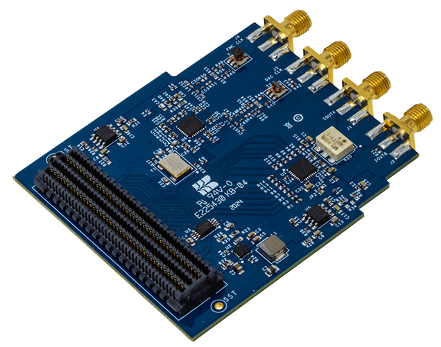
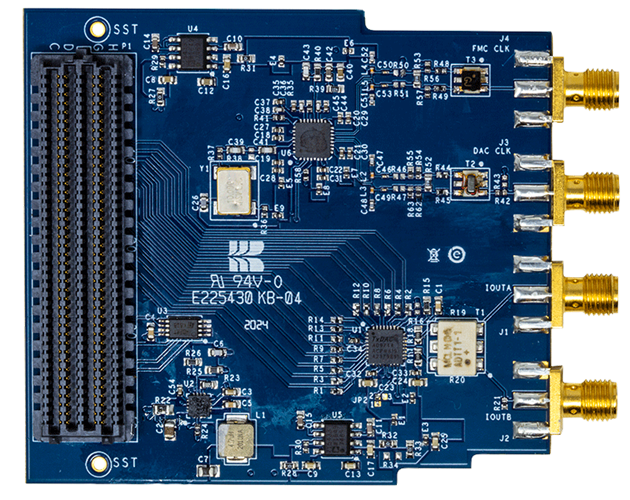
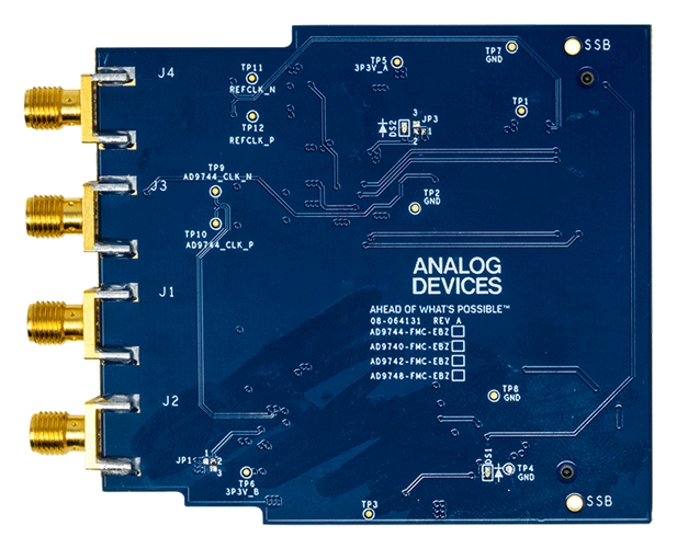
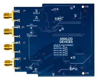
The AD9740ACP-PCBZ/AD9742ACP-PCBZ/AD9744ACP-PCBZ/AD9748ACP-PCBZ evaluation board allows users to easily set up and test the 32-lead lead frame chip scale package (LFCSP) of the AD9740, AD9742, AD9744, and AD9748 devices. Paying careful attention to layout and circuit design, combined with a prototyping area, allows the user to effectively evaluate the AD9740, AD9742, AD9744, and AD9748 in applications that require high resolution and high speed conversion.
The AD9740ACP-PCBZ/AD9742ACP-PCBZ/AD9744ACP-PCBZ/AD9748ACP-PCBZ evaluation board provide flexibility to operate the AD9740, AD9742, AD9744, and AD9748 in various configurations. Possible output configurations include transformer coupled, resistor terminated, and single and differential outputs. The digital inputs are driven from various word generators, and an on-board option can add a resistor network for proper load termination. Users can use the power-down feature of the AD9740, AD9742, AD9744, and AD9748 and can select clock and data modes.
The AD9740, AD9742, AD9744, and AD9748 are wideband, 3G members of the TxDAC® series of high performance, low power CMOS, digital-to-analog converters (DACs). The TxDAC family, consisting of pin-compatible 14-, 12-, 10-, and 8-bit DACs, is specifically optimized for the transmit signal path of communication systems. All the devices share the same interface options, small outline package, and pinout. The AD9740, AD9742, AD9744, and AD9748 also provide an upward or downward component selection path based on performance, resolution, and financial cost. The AD9740, AD9742, AD9744, and AD9748 offer exceptional ac and dc performance while supporting update rates up to 210 MSPS.
The low power dissipation of the AD9740, AD9742, AD9744, and AD9748 makes these devices well suited for portable and low power applications. Lowering the full-scale output current further reduces the power dissipation to 60 mW, with only a slight degradation in performance. Power-down mode also reduces the standby power dissipation to approximately 15 mW. A segmented current source architecture is combined with a proprietary switching technique to reduce spurious components and enhance dynamic performance. Edge triggered input latches and a 1.2 V temperature compensated band gap reference are integrated to provide a complete, monolithic DAC solution. The digital inputs support 3 V logic families.
For more information about the AD9740, AD9742, AD9744, and AD9748, refer to the corresponding data sheets. Consult the data sheets in conjunction with this user guide when using the AD9740ACP-PCBZ/AD9742ACP-PCBZ/AD9744ACP-PCBZ/AD9748ACP-PCBZ evaluation board.
Applicable Parts
Documentation & Resources
-
AD974x-ACP-PCBZ - User Guide (Rev. A)4/9/2021PDF1 M
-
AD974x-FMC-EBZ User Guide4/9/2021WIKI
-
SDP-H1 for High-Speed DAC Evaluation4/9/2021WIKI
-
UG-502: SDP-H1 Controller Board4/5/2013PDF1896 kB
-
PCB Layout4/9/2021PDF
-
Schematic4/9/2021PDF
-
BRD File4/9/2021BRD
-
BOM4/9/2021CSV
-
PCB Layout Top2/4/2020PDF
-
PCB Layout Bottom2/4/2020PDF
-
Schematic2/4/2020PDF
-
BOM2/4/2020PDF
