Layout Guidelines with Example Layout for the MAX20021/MAX20022
Abstract
This application note explains how to layout the MAX20021/MAX20022 automotive quad power-management ICs (PMICs) to maximize performance and minimize emissions. Example images of a four-layer layout are provided.
Introduction
Good PCB layout is essential, especially when using a high-frequency switching regulator such as the MAX20021 or the MAX20022. An optimized layout provides a clean output supply and saves time debugging emissions issues in the electromagnetic interference (EMI) chamber. This application note outlines some critical areas of the circuit where optimizing the layout provides the most benefit.
General Layout Guidelines
- Minimize the trace loop area for the input capacitor (C5–C8), inductor (L1–L4), and output capacitor (C1–C4) for each output.
- Place the VA output capacitor (C9) as close as possible to pin 26 (VA) and pin 24 (GND) without any vias between the pins and the capacitor. This is the analog supply for the IC; any inductance on this connection increases noise on the analog supply, which can, in turn, increase jitter on the LX[1:4] outputs.
- A shorter trace is better than a wider trace.
Optimizing the AC-DC Current Path
To minimize emissions, the layout of the passive components of the MAX20021/MAX20022 is critical. The paths where there are current-step changes are considered the AC current paths. These AC current paths can be seen by eliminating the paths where current flows on both the ON and OFF parts of the switching cycle. The paths that have current flowing through them during the ON and OFF cycles are considered the DC current paths.
AC Current Path
The MAX20021 synchronous DC-DC converter has three passive components (C1, C5, L1) for each output directly in the switching current path. These three components have the most impact on emissions and device performance. Figures 1 and 2 show the switching current path during the ON and OFF cycles for OUT1; Figure 3 shows the difference between these two current paths where the highest di/dt occurs. Optimizing the layout of component C5 is the highest priority, followed by optimizing for L1 and C1.
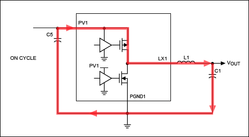
Figure 1. OUT1 current flow with PMOS ON.

Figure 2. OUT1 current flow with DMOS ON.

Figure 3. OUT1 AC current flow showing difference.
Spread Spectrum
When a good layout is not enough to pass customer-required emissions tests, the MAX20021/MAX20022 can be ordered with spread-spectrum clock enabled. The spread-spectrum-enabled device can reduce the FM-band noise by as much as 12dB over the standard version. See the data sheet for information on how to order the spread-spectrum-enabled versions.
Example: Four-Layer PCB Layout
Figures 4 through 7 show an example of a four-layer layout using the guidelines above.

Figure 4. Example of a four-layer PCB layout—top layer.

Figure 5. Example of a four-layer PCB layout—PGND layer.
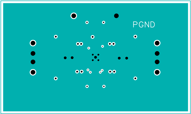
Figure 6. Example of a four-layer PCB layout—VSUP layer.
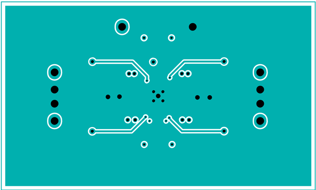
Figure 7. Example of a four-layer PCB layout—bottom layer.
Conclusion
Proper layout of the critical passive components for the switching regulators of the MAX20021/MAX20022 (Figure 8) helps to minimize noise and emissions at the source. This saves valuable time and effort during the qualification phase of the project.
| Designation |
Qty | Description |
| C1–C4 |
4 | 10µF, 10V ±10% X7R 1206 ceramic capacitor |
| C5–C8 |
4 | 2.2µF, 10V ±10% X7R 0603 ceramic capacitor |
| C9 |
1 | 470nF, 10V ±10% X7R 0402 ceramic capacitor |
| R1–R4 |
1 | 20kΩ ±1% 0402 resistors |
| L1–L4 |
4 | MTD2520–CN1R5M 1.5µH inductor |
| U1 | 1 | MAX20021/MAX20022 quad, low-voltage DC-DC converters |

Figure 8. Schematic diagram used for PCB layout.