AN-2615: Upgrading GMSL2 to GMSL3
Abstract
This article details the design considerations when upgrading an existing GMSL2™ design to a GMSL3™ design. The specific examples use a GMSL2 sensor pair, the MAX96717 and MAX96716A, and a pin-for-pin compatible GMSL3 sensor pair, the MAX96793 and MAX96792A. The article covers the benefits of GMSL3 along with design considerations for upgrading from GMSL2 to GMSL3.
Introduction
One of the primary benefits of the GMSL™ technology is the intergeneration compatibility between devices within one generation. GMSL2 is backwards compatible with GMSL1™ and GMSL3 is backwards compatible with GMSL2; verify the part’s compatibility by using the data sheet. This flexibility also translates to time savings by maintaining the same pin and package to reuse designs for compatible parts.
GMSL3 Overview
The main difference with GMSL3 is doubling the GMSL data rate on the link up to 12Gbps. GMSL2 is typically sufficient for most applications, however, sensor and display bandwidths continue to increase. GMSL3 aims to achieve these higher data rates while maintaining all the benefits of GMSL, including adaptive equalization (AEQ), ASIL-B functional safety, and robust error monitoring diagnostics.
GMSL2 uses non-return to zero (NRZ) modulation which has a Nyquist frequency of half the transmission data rate. This translates to 3GHz for a 6Gbps link (or 1.5GHz for a 3Gbps link). Doubling the data rate while still using NRZ modulation translates to 6GHz for a 12Gbps link. However, there are disadvantages for using this higher frequency such as more insertion loss on the cable, connector, and PCB to reduce the total cable length of the application.
To avoid a higher frequency for double the data rate, GMSL3 leverages pulse-amplitude modulation 4 level (PAM4) to maintain the same Nyquist frequency as GMSL2. The lower operating frequency on the channel delivers many system benefits:
- GMSL2 and GMSL3 utilize the same clock link rate for schematic and layout reuse, operating on FR-4 PCBs.
- There is lower insertion loss on cables and connectors.
- Higher spectral efficiency by doubling the bandwidth and maintaining the same link rate.
The GMSL3 supports both 6Gbps with NRZ and 12Gbps with PAM4.
Design Considerations
To demonstrate, consider the MAX96793 CSI-2 to GMSL3 serializer and the MAX96792A GMSL3 to CSI-2 deserializer. In general, the changes are minimal but need to be reviewed for each system application.
Pin-for-Pin Compatibility
GMSL devices between GMSL2 and GMSL3 generations are designed to be pin-for-pin compatible for design reuse. The serializer packages are 5mm x 5mm TQFN devices. Figure 1 details the pinouts of the MAX96717 and MAX96793:


When using the reference clock over reverse (RoR) capability on these devices, connect a 20nF± 10% capacitor between the VREF pin (pin 7) and ground. This connection is required for GMSL3 mode when using RoR and optional for GMSL2 mode to maintain optimal reverse link margin.
If RoR is not being used on GMSL3, this capacitor is not required.
The deserializer packages are 7mm x 7mm TQFN devices. Figure 2 details the pinouts of the MAX96716A and MAX96792A:


Power Consumption
Power consumption of these devices is characterized by using the physical layer interfaces to their full, operational capacity as detailed in the Configuration column of Table 1.
| DEVICE | CONFIGURATION | IDD18 | IDD (VDD = 1.2V) | PTOTAL |
| MAX96717 | 6Gbps Forward Link Rate (GMSL2 Mode) RGB888 Color Bar Pattern 4-lane CSI-2 DPHY input 1.3Gbps per lane |
46mA (25°C) 53mA (105°C) |
98mA (25°C) 232mA (105°C) |
~210mW (25°C) ~393mW (105°C) |
| MAX96793 | 12Gbps Forward Link Rate (GMSL3 Mode) RGB888 Color Bar Pattern 4-lane CSI-2 DPHY input 2.5Gbps per lane |
46mA (25°C) 53mA (105°C) |
170mA (25°C) 340mA (105°C) |
~301mW (25°C) ~529mW (105°C) |
Both devices utilize the same power supply rail voltages to simplify power-supply topology requirements. The VDD18 rail uses the same power for both of the MAX96717 and MAX96793 GMSL device families. The maximum current on VDD core rail has only a slight current increase of approximately ~70mA (25°C) or ~110mA (105°C). Check the powersupply source to ensure there is enough margin on the rail to accommodate the current increase.
As previously mentioned, these devices are characterized by a configuration intended to use the physical layer interfaces to their fullest capacity, which translates to both GMSL inputs and both MIPI-CSI2 outputs for the deserializer. These devices can be used with a single GMSL input and/or a single MIPI-CSI2 output to reduce total power consumption.
Additionally, the camera deserializer devices have a MIPI-CSI2 supply rail VTERM for the MIPI-CSI2 PHY.
| DEVICE | CONFIGURATION | IDD18 | IDD (VDD = 1.2V) | ITERM | PTOTAL |
| MAX96716A | 6Gbps Forward Link Rate (GMSL2 Mode) 2x 6Gbps inputs 2x 4-Lane CSI-2 DPHY inputs 1.3Gbps per lane |
196mA (25°C) 245mA (105°C) |
197mA (25°C) 460mA (105°C) |
27mA (25°C) 40mA (105°C) |
~654mW (25°C) ~1095mW (105°C) |
| MAX96792A | 12Gbps Forward Link Rate (GMSL3 Mode) 2x 12Gbps inputs 2x 4-Lane CSI-2 DPHY inputs 2.5Gbps per lane |
210mA (25°C) 250mA (105°C) |
365mA (25°C) 850mA (105°C) |
31mA (25°C) 40mA (105°C) |
~898mW (25°C) ~1596mW (105°C) |
Both devices utilize the same power-supply rail voltages to simplify the power-supply topology requirements. The VDD18 rail uses approximately the same power for both of the MAX96716A and MAX96792A GMSL device families. The maximum current on VDD core rail has a current increase of approximately ~160mA (25°C) or ~390mA (105°C). Check the power-supply source to ensure there is enough margin on the rail to accommodate the current increase.
Additionally, the quiescent current draw and the maximum power-supply noise tolerance is the same for both devices to maintain the same system requirements for both families.
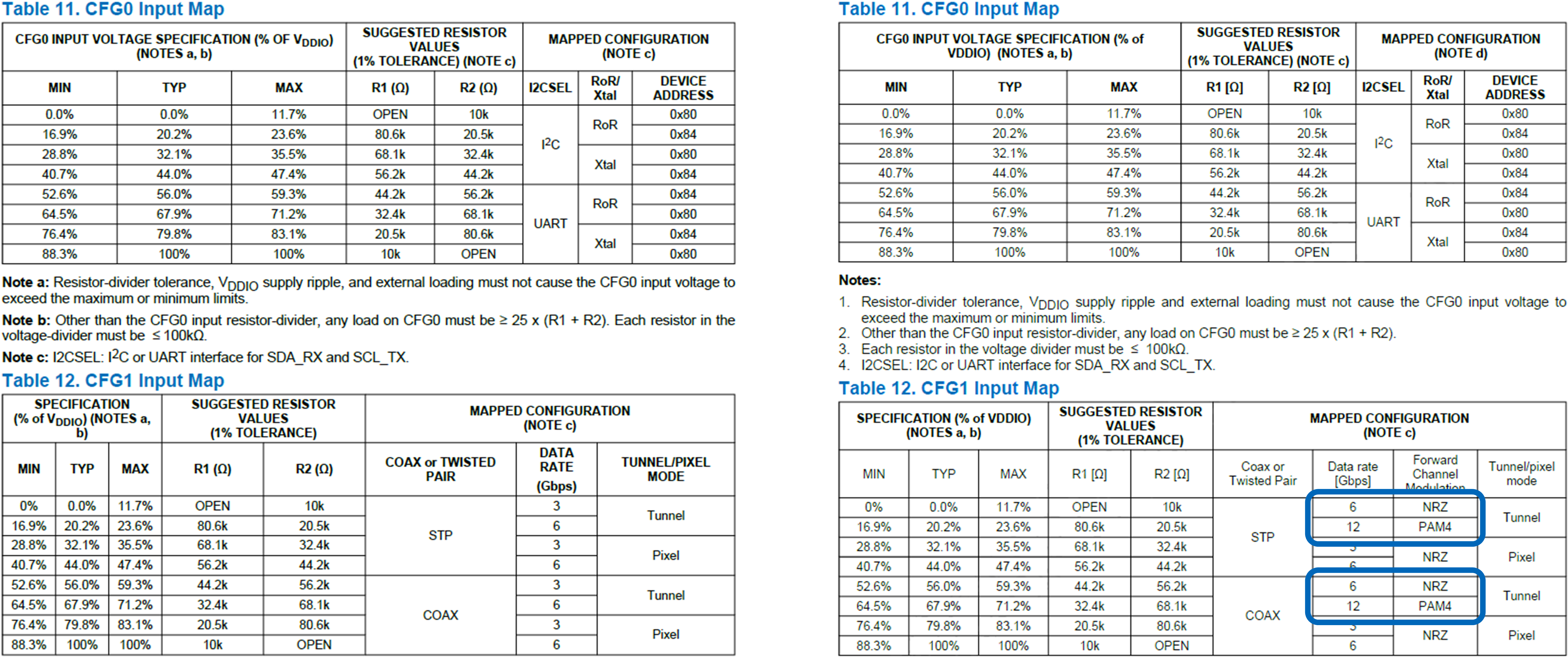
Configuration Pin Settings
The configuration pins for these devices have only a few differences. It is important to confirm the configuration pin values from the device data sheet as these will determine how the devices will be configured at every bootup.
Figure 3 and Figure 4 show the details of the configuration pins, which are specific to the MAX96717 and MAX96793 for the sake of explanation. All configuration pin settings are device specific and detailed in their respective device data sheets.
Configuration 0 pin (CFG0) configures the communication channel interface between UART and I2C, the option to use RoR or crystal, and the device address.
Configuration 1 pin (CFG1) configures the cable type of STP or coax, the GMSL data rate, and the choice of tunnel or pixel mode. CFG1 has the minor differences for setting the GMSL data rate. The pixel mode data rates are the same between devices. The tunnel mode operation supports 6Gbps and 12Gbps for GMSL3 and 3Gbps and 6Gbps for GMSL2.


PAM4 Modulation Scheme
Scheme PAM4 is an existing modulation scheme that GMSL leverages for rigorous automotive environments. Where NRZ uses two voltage levels to represent a 1-bit symbol, PAM4 uses four voltage levels to represent a 2-bit symbol to allow GMSL3 to operate at the same baud rate as GMSL2 and double the bit rate of data transmitted.
Doubling the data rate, however, is not without consequences; the tradeoff is that PAM4 has a smaller eye opening that is approximately 1/3 of the NRZ eye opening.


In Figure 5, ‘A’ is defined as the NRZ eye opening, which means that if NRZ transmits 1 bit per period (1/T) with an SNR of A, then PAM4 transmits 2 bits per period (2/T) with an SNR of A/3.
Forward Error Correction
To overcome this noise sensitivity inherent with PAM4, GMSL3 includes forward-error correction (FEC) to add data redundancy and error correction capabilities to the link. FEC can significantly reduce the SNR requirement and helps decrease the bit error rate (BER) of the link to essentially one bit error for the lifetime of the GMSL link.
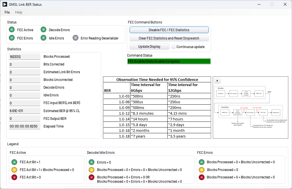
GMSL FEC utilizes Reed-Solomon encoding, which is found in CDs, QR codes, and even the Voyager spacecraft [1]. Additionally, this FEC information can be monitored in real time with registers or conveniently in the GMSL GUI.

Since FEC is mandatory for GMSL3 operation, the bandwidth impact needs to be factored in when confirming a use case has sufficient bandwidth. Using FEC consumes an additional 6.67% (128/120) on the GMSL link for the added BER robustness. The GMSL bandwidth calculator in the GMSL GUI includes this overhead in the calculation. This overhead translates to approximately ~9.7Gbps of useable bandwidth on the GMSL3 link.


Error Reporting
When using FEC on the GMSL3 link, a different error monitoring ideology is required based on the system monitoring requirements. FEC allows for detecting and correcting errors that may occur on the link so it is possible to have FEC correctable bits since the devices report the corrections. FEC uncorrectable bits are not allowed, which indicates that the GMSL3 device is unable to correct an error that occurred on the link.
As a result, error monitoring needs to be adjusted depending on what is deemed an error. For GMSL2 mode, decode and idle errors are used to report errors occurring on link. For GMSL3 mode, FEC uncorrectable errors are used to report errors on the link; FEC corrected bits are also reported.
By default, the FEC error flag checks correctable and uncorrectable bits and reports to ERRB pin. The FEC threshold for correctable bits must be adjusted to the system requirements. Error monitoring changes are detailed in the software differences section.
Channel Specification
A significant change between GMSL2 and GMSL3 is the GMSL channel specification. Do not assume that a compliant GMSL2 system is compatible with the GMSL3 channel specification due to the stricter budget. Refer to the latest GMSL2 channel specification and GMSL3 channel specification available on analog.com.
It is important to reevaluate PCB layouts and cabling needs when reusing designs.
GMSL3 (12Gbps) and GMSL2 (6Gbps) both operate with a fundamental 3GHz link frequency.
GMSL3 insertion loss requirements are additionally specified with both a long channel (high loss) and short channel (low loss). A short channel has a tighter insertion loss (IL), but a relaxed return loss (RL).
GMSL3 return loss requirements are additionally specified with both a long channel (high loss) and a short channel (low loss). A short channel has a relaxed RL, but a tighter IL.
The S-parameter data must be filtered before comparing it to the GMSL3 IL and RL limits. A 100MHz filter is applied to the S-parameters across the full range. Apply unfiltered data from the lowest captured frequency up to 50MHz. Beyond 50MHz, use filtered data to compare to the limit.
Register Settings Difference
There are two main software differences between these devices: operating in GMSL3 mode and error monitoring.
For GMSL3 mode, all the following changes detailed in Table 3 and Table 4 are handled through the CFG pins. These pins correctly configure the device’s transmit and receive speed along with the PAM4 modulation. Table 3 and Table 4 identify the registers in case the software is programming or overriding the CFG pins, which is not typically recommended.
Note: If using CFG pins to configure the GMSL mode, the following changes shown in Table 3 and Table 4 are not required.
The programming procedure needs to be performed in a specific order. Start with the remote device, then follow with the local device. Remote and local terminology refer to the location of the I2C controller. Programming the local device prevents communication to the remote device. For this example, the MAX96793 is the remote device and the MAX96792A (which is connected to the I2C controller) is the local device.
| STEP | LOCATION | DEVICE | DESCRIPTION | REGISTER | VALUE |
| 1 | Remote | MAX96793 | Change Tx rate to 12Gbps | 0x0001 | REG1[3:2] = 0b11 |
| 2 | Remote | MAX96793 | Enable FEC | 0x0028 | TX0[1] = 0b1 |
| 3 | Remote | MAX96793 | Disable GMSL2 mode and enable GMSL3 mode | 0x0006 | REG6[7] = 0b0 |
| 4 | Local | MAX96792A | Hold the GMSL link in RESET | 0x0010 | CTRL0[6] = 0b1 |
| 5 | Local | MAX96792A | Change Rx rate to 12Gbps | 0x0001 | REG1[1:0] = 0b11 |
| 6 | Local | MAX96792A | Enable FEC | 0x0028 | TX0[1] = 0b1 |
| 7 | Local | MAX96792A | Disable GMSL2 mode and enable GMSL3 mode | 0x0004 | REG4[7:6] = 0b11* |
| 8 | Local | MAX96792A | Release the GMSL link from RESET | 0x0010 | CTRL0[6] = 0b0 |
| *This sets both links to GMSL3. Each link can be configured individually. | |||||
| STEP | LOCATION | DEVICE | DESCRIPTION | REGISTER | VALUE |
| 1 | Remote | MAX96793 | Change Tx rate to 6Gbps | 0x0001 | REG1[3:2] = 0b10 |
| 2 | Remote | MAX96793 | Disable FEC | 0x0028 | TX0[1] = 0b0 |
| 3 | Remote | MAX96793 | Enable GMSL2 mode and disable GMSL3 mode | 0x0006 | REG6[7] = 0b0 |
| 4 | Local | MAX96792A | Hold the GMSL link in RESET | 0x0010 | CTRL0[6] = 0b1 |
| 5 | Local | MAX96792A | Change Rx rate to 6Gbps | 0x0001 | REG1[1:0] = 0b10 |
| 6 | Local | MAX96792A | Disable FEC | 0x0028 | TX0[1] = 0b0 |
| 7 | Local | MAX96792A | Enable GMSL2 mode and disable GMSL3 mode | 0x0004 | REG4[7:6] = 0b00* |
| 8 | Local | MAX96792A | Release the GMSL link from RESET | 0x0010 | CTRL0[6] = 0b0 |
| *This sets both links to GMSL3. Each link can be configured individually. | |||||
As mentioned in the Error Reporting section, the error monitoring ideology does need to change depending on the FEC reporting.
| MAX96793 | MAX96792A | |||
| BIT NAME | REGISTER | VALUE | REGISTER | VALUE |
| DEC_ERR_OEN_A | 0x001A | INTR2[0] = 0b1 | 0x001A | INTR2[0] = 0b1 |
| DEC_ERR_OEN_B | — | — | 0x001A | INTR2[1] = 0b1 |
| IDLE_ERR_OEN | 0x001A | INTR2[2] = 0b1 | 0x001A | INTR2[2] = 0b1 |
| IDLE_ERR_OEN_B | — | — | 0x5010 | INTR10[6] = 0b1 |
| FEC_RX_ERR_OEN | — | — | 0x001C | INTR4[5] = 0b0* |
| FEC_RX_ERR_OEN_B | — | — | 0x5010 | INTR10[5] = 0b0* |
| *Each link can be configured individually. | ||||
| MAX96793 | MAX96792A | |||
| BIT NAME | REGISTER | VALUE | REGISTER | VALUE |
| DEC_ERR_OEN_A | 0x001A | INTR2[0] = 0b0 | 0x001A | INTR2[0] = 0b0 |
| DEC_ERR_OEN_B | — | — | 0x001A | INTR2[1] = 0b0 |
| IDLE_ERR_OEN | 0x001A | INTR2[2] = 0b0 | 0x001A | INTR2[2] = 0b0 |
| IDLE_ERR_OEN_B | — | — | 0x5010 | INTR10[6] = 0b0 |
| FEC_RX_ERR_OEN | — | — | 0x001C | INTR4[5] = 0b1* |
| FEC_RX_ERR_OEN_B | — | — | 0x5010 | INTR10[5] = 0b1* |
| *Each link can be configured individually. | ||||
With FEC enabled, the FEC statistics can be configured individually for the applications requirements. There is an abundance of registers for the MAX96792A, which starts at register block address 0x2000 to read the statistics and set error thresholds for both links.
For example, your application may allow for a certain number of correctable bit errors before raising alarm so set the CORRECTED_THRESHOLD_0/1/2/3 to the permitted number of corrected bits. Uncorrectable bit errors are more concerning and indicate a greater problem in the system.
The breadth of statistics allows for a comprehensive GMSL link state of health.
Conclusion
The GMSL2 and GMSL3 device families are designed to grow with designs and the details outlined show the changes to consider when upgrading a system. In general, GMSL2 and GMSL3 devices remain as consistent as possible to alleviate the design burden when upgrading. As two specific device upgrades are detailed in this article, it is mandatory to review the documentation of any additional GMSL2 and GMSL3 devices for the design. However, GMSL bandwidth calculations and GMSL channel specifications remain consistent for all GMSL devices.
References
[1] Canterbury, “QR codes - Coding - Error control - Computer Science Field Guide,” Csfieldguide.org.nz, 2024. https://www.csfieldguide.org.nz/en/chapters/coding-error-control/qr-codes.