AN-1527: Creating a Constant Envelope Signal Using the ADL5331 RFVGA and AD8319 Log Detector
Circuit Function and Benefits
Overall performance of a transmitter, wired or wireless, is a strong function of the output power of the amplifier. If the signal is weak, bit error rate (BER) or modulation error rate (MER) degrades due to low signal-to-noise ratio (SNR). If the signal is too strong, distortion causes the same issues. The circuit shown in Figure 1 uses the ADL5331 variable gain amplifier (VGA), the AD8319 power detector, and the AD5621 low power nanoDAC® to generate output power control accurate to 12 bits.


The AD8319 has high temperature stability to compensate for any gain variation over temperature of the VGA, resulting in accurate power control over a wide temperature range. Because the AD8319 control input, VSET, and output, VOUT, are related to the radio frequency (RF) input on a volts/dB scale and the AD5621 nanoDAC has a linear transfer function, the resulting output power control is linear in dB vs. digital-to-analog converter (DAC) input code.
Circuit Description
The ADL5331 VGA provides accurate gain control. However, an automatic gain control (AGC) achieves a more precise regulation of output power. Figure 1 shows the ADL5331 operating in an AGC loop. The addition of the AD8319 logarithmic amplifier allows the AGC to have improved temperature stability over a wide output power control range.
To operate the ADL5331 VGA in an AGC loop, a sample of the output RF is back to the detector (typically using a directional coupler and additional attenuation). A setpoint voltage is applied by the AD5621 DAC to the VSET input of the detector while VOUT is connected to the GAIN pin of the ADL5331. Based on the defined linear in dB relationship of the detector between VOUT and the RF input signal, the detector adjusts the voltage on the GAIN pin (the VOUT pin of the detector is an error amplifier output) until the level at the RF input corresponds to the applied setpoint voltage. The GAIN pin settles to a value that results in the correct balance between the input signal level at the detector and the setpoint voltage.
The basic connections for operating the ADL5331 in an AGC loop with the AD8319 are shown in Figure 1. The AD8319 is a 1 MHz to 10 GHz precision demodulating logarithmic amplifier. It offers a dynamic detection range of 40 dB with ±1 dB temperature stability. The VOUT pin of the AD8319 controls the gain control pin, GAIN, of the ADL5331. In this application, when the AD8319 is in controller mode, the VOUT pin of the AD8319 can drive the ADL5331 GAIN pin over its full linear range of 0 V to 1.4 V. Under low power RF input conditions, outside the linear control range of the loop, the VOUT pin of the AD8319 can be driven to its maximum value, close to the value of the positive input voltage, VPOS. To avoid overdrive recovery issues with the ADL5331 GAIN input, place a voltage divider between VOUT on the AD8319 and GAIN on the ADL5331. This can have a slight effect on the overall speed of the loop, for instance, when the input power to the ADL5331 is stepped.
A coupler with an attenuation of 23 dB matches the desired output power range from the VGA to the linear operating range of the AD8319. In this case, the desired output power range of the VGA is −15 dBm to +15 dBm. With the given coupler and attenuation, the range of power to the AD8319 RF input is −8 dBm to −38 dBm, within the specified range of −3 dBm to −43 dBm for a ±1 dB error.
The error amplifier of the detector uses a ground referenced capacitor pin, CLFP, to integrate the error signal in the form of a current. Connect a capacitor to the CLFP pin to set the loop bandwidth and to ensure loop stability.
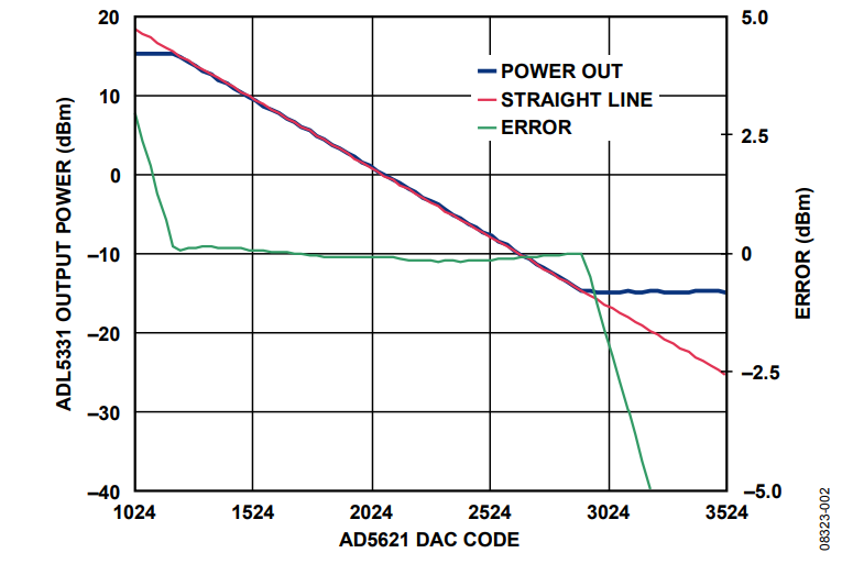
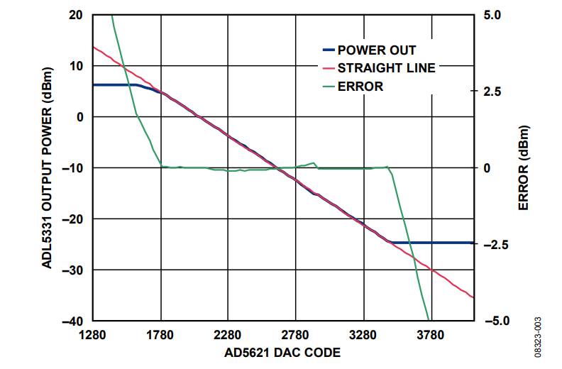
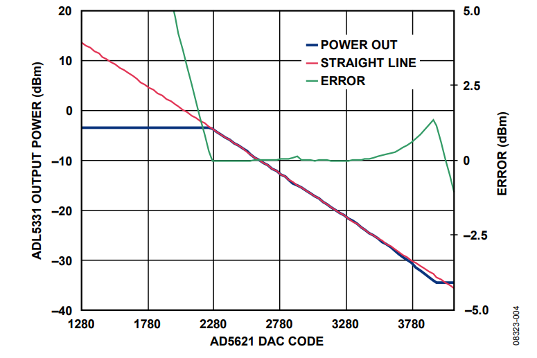
Figure 2, Figure 3, and Figure 4 show the transfer function of the ADL5331 output power vs. the AD5621 DAC code for a 100 MHz sine wave with an input power of 0 dBm, −10 dBm, and −20 dBm. The power control of the AD8319 has a negative sense. Decreasing the DAC code, which corresponds to demanding a higher signal from the ADL5331, increases the gain.


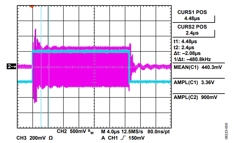
For the AGC loop to remain in equilibrium, the AD8319 must track the envelope of the ADL5331 output signal and provide the necessary voltage levels to the gain control input of the ADL5331. Figure 5 shows an oscilloscope measurement of the AGC loop in Figure 1. A 100 MHz sine wave with 50% amplitude modulation (AM) is applied to the ADL5331. The output signal from the ADL5331 is a constant envelope sine wave with amplitude corresponding to a setpoint voltage at the AD8319 of 1.5 V. The gain control response of the AD8319 to the changing input envelope is also shown in Figure 5.

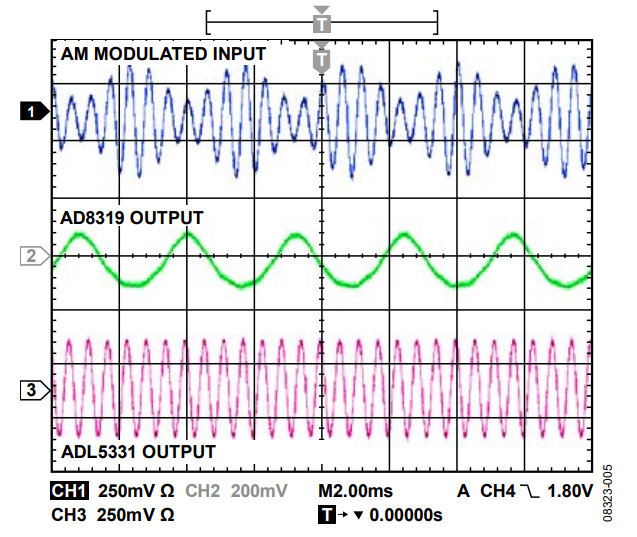
Figure 6 shows the response of the AGC RF output to a pulse on the VSET pin. As the VSET pin decreases to 1 V, the AGC loop responds with an RF burst. Response time and the amount of signal integration are controlled by the capacitance at the AD8319 CLFP pin. This function is analogous to the feedback capacitor around an integrating amplifier. An increase in the capacitance results in a slower response time.

Construct the circuit on a multilayer printed circuit board (PCB) with a large area ground plane. Use proper layout, grounding, and decoupling techniques to achieve optimum performance (see MT-031, MT-101, and the EVAL-ADL5331 and EVAL-AD8319 evaluation board layouts).
On the bottom of the ADL5331 and AD8319 chip scale packages, there are exposed compressed paddles. These paddles are internally connected to the ground of the chips. Solder the paddles to the low impedance ground plane on the PCB to ensure the specified electrical performance and to provide thermal relief. It is also recommended that the ground planes on all layers under the paddle be stitched together with vias to reduce thermal impedance.
Common Variations
This circuit can implement a constant power out function (fixed setpoint with variable input power) or a variable power out function (variable setpoint with fixed or variable input power). If a higher output power control range is desired, the AD8318 logarithmic amplifier (60 dB power detection range) can be used in place of the AD8319. For a constant output power function, the lower dynamic range of the AD8319 is adequate because the loop always servos the input power of the detector to a constant level.
The ADL5331 VGA, which is optimized for transmit applications, can also be replaced by the AD8368 VGA. The AD8368 is optimized for low frequency receive applications up to 800 MHz and provides 34 dB of linear in dB, voltage controlled variable gain.
References
MT-073 Tutorial, High Speed Variable Gain Amplifiers. Analog Devices.
MT-077 Tutorial, Log Amp Basics. Analog Devices.
MT-078 Tutorial, High Speed Log Amps. Analog Devices.