AN-1524: USB-Based Temperature Monitor Using the ADuC7061 Precision Analog Microcontroller and an External RTD
AN-1524: USB-Based Temperature Monitor Using the ADuC7061 Precision Analog Microcontroller and an External RTD
Circuit Function and Benefits
This circuit shows how the ADuC7061 precision analog micro-controller can be used in an accurate resistance temperature detector (RTD) temperature monitoring application. The ADuC7061 integrates dual, 24-bit, Σ-Δ, analog-to-digital converters (ADCs), dual programmable current sources, a 14-bit digital-to-analog converter (DAC), and a 1.2 V internal reference, as well as an ARM7TDMI® core, 32 kB Flash/EE, 4 kB SRAM, and various digital peripherals such as UART, timers, serial peripheral interface (SPI), and I2C interfaces. The ADuC7061 is connected to a 100 Ω RTD.
In the source code, an ADC sampling rate of 100 Hz is chosen. When the ADC input programmable gain amplifier (PGA) is configured for a gain of 32. The noise free code resolution of the ADuC7061 is greater than 18 bits.
Circuit Description
The circuit shown in Figure 1 is powered entirely from the USB interface. The 5 V supply from the USB is regulated to 2.5 V using the ADP3333 2.5 V low dropout (LDO) linear regulator. The regulated 2.5 V supplies the DVDD voltage to the ADuC7061. The AVDD supply to the ADuC7061 has additional filtering as shown in Figure 1. A filter is also placed on the USB supply at the input of the linear regulator.

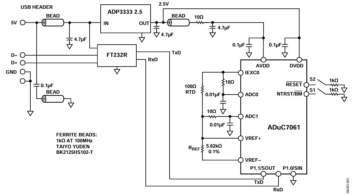
The following features of the ADuC7061 are used in this application:
- Primary 24-bit Σ-Δ ADC with PGA: The PGA is set for a gain of 32 in the software for this application.
- Programmable excitation current sources for forcing a controlled current through the RTD. The dual current sources are configurable in 200 µA steps from 0 µA to 2 mA. For this example, a 200 µA setting was used.
- External voltage reference for the ADC in the ADuC7061. For this application, a ratiometric setup was used where an external reference resistor (RREF) is connected across the external VREF+ and VREF− pins. Alternatively, an internal 1.2 V reference is provided in the ADuC7061.
- ARM7TDMI core. The powerful 16-bit/32-bit ARM7 core with integrated 32 kB Flash/EE and SRAM memory runs the user code that configures and controls the ADC, processes the ADC conversions from the RTD, and controls the communications over the UART/USB interface.
- UART. The UART is the communication interface to the host PC.
- Two external switches force the device into its flash boot mode. By holding S1 low and toggling S2, the ADuC7061 enters boot mode instead of normal user mode. In boot mode, the internal flash can be reprogrammed through the UART interface.
The RTD used in the circuit is a platinum 100 Ω RTD, model number Enercorp PCS_1.1503.1. It is available in a 0805 surface-mount package. This RTD has a temperature variation of 0.385 Ω/°C.
Note that the reference resistor, RREF, should be a precision 5.62 kΩ (±0.1%).
The USB interface to the ADuC7061 is implemented with an FT232R UART to USB transceiver, which converts USB signals directly to the UART.
In addition to the decoupling shown in Figure 1, the USB cable itself should have a ferrite for added electromagnetic interference (EMI)/radio frequency interference (RFI) protection. The ferrite beads used in the circuit were Taiyo Yuden, BK2125HS102-T, which have an impedance of 1000 Ω at 100 MHz.
The circuit must be constructed on a multilayer printed circuit board (PCB) with a large area ground plane. Proper layout, grounding, and decoupling techniques must be used to achieve optimum performance (see MT-031, Grounding Data Converters and Solving the Mystery of "AGND" and "DGND," MT-101, Decoupling Techniques, and the EVAL-ADuC7061 evaluation board layout).
Code Description
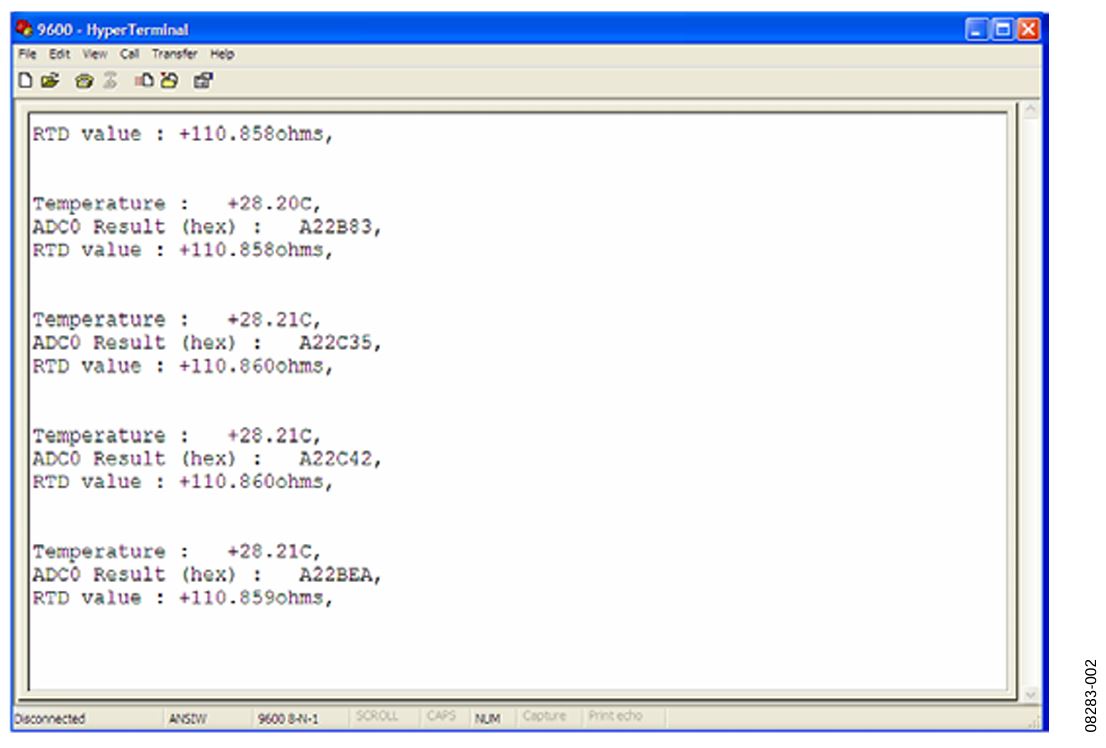
The UART is configured for a baud rate of 9,600, 8 data bits, no parity, and no flow control. If the circuit is connected directly to a PC, use a communication port viewing application such as HyperTerminal® to view the results sent by the program to the UART (see Figure 2). The source code is commented to make it easier to understand and manipulate.

For details on linearization and maximizing the performance of the circuit, refer to Application Note AN-0970, RTD Interfacing and Linearization Using an ADuC706x Microcontroller.
Common Variations
The ADP7102 LDO regulator can be used as an alternative to the ADP3333. If more GPIO pins are required on the microcontroller, the ADuC7060, which comes in a 48-lead LFCSP or 48-lead LQFP package, is another option. Note that the ADuC7060/ADuC7061 can be programmed or debugged via a standard JTAG interface. For a standard UART to RS-232 interface, the FT232R transceiver can be replaced with the ADM3202, which requires a 3 V power supply.
References
Kester, Walt. 1999. Sensor Signal Conditioning. Analog Devices. Section 4, "Temperature Sensors."
MT-022 Tutorial, ADC Architectures III: Sigma-Delta ADC Basics. Analog Devices.