AN-1520: Low Cost Differential Video Receiver Using the ADA4851-1 Amplifier and the ADV7180 Video Decoder
Circuit Function and Benefits
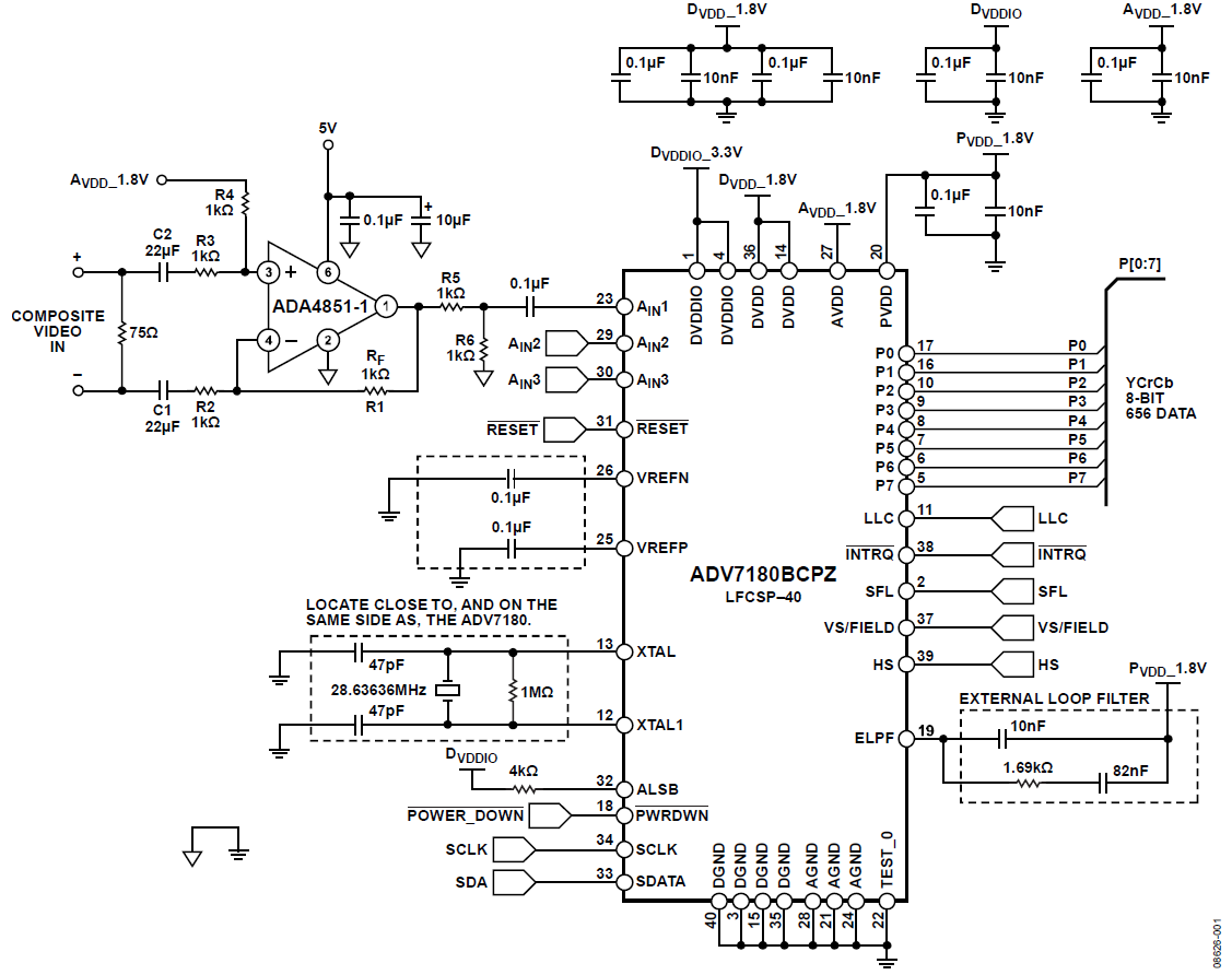
The circuit described in this document and shown in Figure 1 provides a low cost, low power, unipolar, differential receiver using the ADA4851-1 for an incoming video signal before the video signal is digitized by the ADV7180 video decoder. This circuit eliminates common-mode noise and phase noise caused by ground potential difference from an incoming video signal and is well suited for automotive infotainment and vision safety systems.

(Simplified Schematic: Decoupling and All Connections Not Shown)
The ADA4851-1 family of amplifiers along with the ADV7180 video decoder are all automotive qualified, which makes both products ideal for auto-vision applications. Low power, low cost, high speed, and fast settling make these amplifiers well suited for many video applications in which these requirements are important. Figure 1 shows only a single amplifier for simplicity; the amplifier circuit can be repeated for each input as many times as needed.
Circuit Description
The ADA4851-1 is a single (also available as a dual or quad amplifier in a single package), 130 MHz, low power, low cost, high speed, voltage feedback, rail-to-rail output amplifier that has an operating supply range of 3 V to 5 V. In Figure 1, the ADA4851-1 is configured as a low cost differential to single-ended receiver for video signals.
This configuration is a standard four-resistor difference amplifier optimized for composite video frequencies, with a differential to single-ended gain of 1. The amplifier only amplifies the difference between the two inputs, while eliminating the common-mode noise between the incoming signals and allowing the reconstruction of the original signal. Using low value, high accuracy resistors and a high common-mode rejection ratio (CMRR) amplifier provides the exceptional performance.
A critical design consideration that is important to note about this architecture is its dependence on resistor matching for the common-mode rejection (CMR) of this circuit design. The CMR can be calculated using the following formula:

where KR is a single resistor tolerance in fractional form (for example, 1% = 0.01).
It is assumed that the amplifier has significantly higher CMR performance. This formula shows that if 54 dB or better CMR is desired, R1, R2, R3, and R4 must have a matching tolerance of 0.1% or better.
To prevent the incoming signal from violating the amplifier input and output voltage range, it is necessary to add a dc offset. Add a dc offset by connecting R4 to the 1.8 V analog supply voltage (AVDD_1.8V), which is also used by the ADV7180, which helps keep the cost low. To prevent supply noise from coupling into the video signal stream, be sure to have adequate bypassing on this supply (AVDD_1.8V), as shown in Figure 1.
Some automotive applications require ac-coupled inputs to protect the input to the amplifier from a short to a voltage higher than its supply voltage. The input impedance of 1 kΩ (R2 and R3) with the 22 μF capacitors (C1 and C2) sets a high-pass corner frequency pole at approximately 7 Hz. If a lower frequency is desired, increasing the capacitor value decreases the corner frequency proportionally. For example, using 47 μF capacitors results in a 3.4 Hz high-pass corner frequency.
R5 and R6 form a typical voltage divider network that is required to keep the input video signal within the allowed range of the analog-to-digital converter (ADC), 0 V to 1 V. This circuit must be placed before all analog inputs to the ADV7180. If the amplitude of the analog video signal is too high, clipping may occur, resulting in visual artifacts. The voltage divider impedance of can be scaled to help reduce the output power of the ADA4851-1. For high impedance dividers, care must be taken to keep the ADA4851-1 and the ADV7180 very close together, on the printed circuit board (PCB), to reduce the trace parasitic capacitance.
A function that is often overlooked but important is buffering. For example, many automotive customers use low cost amplifiers to protect more expensive and complex devices, such as video decoders and encoders. Amplifiers with ac-coupled inputs, as shown in Figure 1, help protect such devices from overvoltage and electrostatic discharge (ESD) damage.
The ADV7180 automatically detects and converts standard analog baseband television signals compatible with worldwide NSTC, PAL, and SECAM standards into 4:2:2 component video data compatible with the 8-bit ITU-R.656 interface standards. The accurate 10-bit analog-to-digital conversion provides professional quality video performance for consumer applications with true 8-bit data resolution. Three analog video input channels accept standard composite, S-Video, or component video signals, supporting a wide range of consumer video sources. Automatic gain control (AGC) and clamp restore circuitry allow an input video signal peak-to-peak range of up to 1.0 V.
The circuit must be constructed on a multilayer PCB with a large area ground plane. Proper layout, grounding, and decoupling techniques must be used to achieve optimum performance (see the MT-031 Tutorial and MT-101 Tutorial).
Common Variations
If better CMR performance at high frequencies and higher input impedance are desired, the ADA4851-1 can be replaced with the AD8130 differential line receiver.
References
MT-061 Tutorial, Instrumentation Amplifier (In-Amp) Basics, Analog Devices.
MT-068 Tutorial, Difference and Current Sense Amplifiers, Analog Devices.