AN-1511: Programmable Gain Element Using the AD5450/AD5451/AD5452/AD5453 Current Output DAC Family
Circuit Function and Benefits
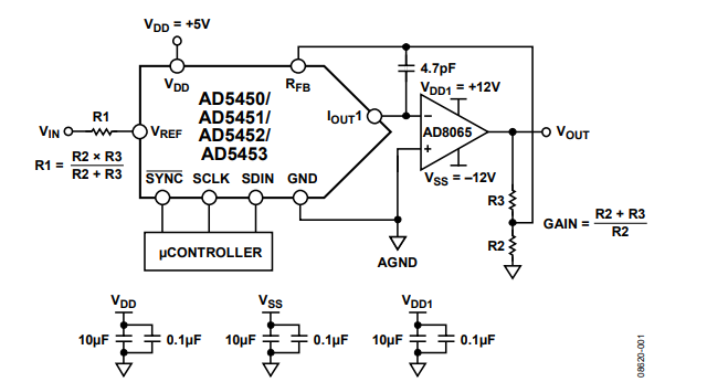
In applications where the digital-to-analog (DAC) output voltage range is required to be larger than the input voltage, use a programmable gain circuit. This circuit provides a programmable gain function using a multiplying DAC, the AD5450/AD5451/AD5452/AD5453, and a fast, low offset operational amplifier, the AD8065. External resistors set the maximum gain value and the temperature coefficient, and the DAC resolution sets the programmable gain.

Circuit Description
The circuit shown in Figure 1 is the recommended method of increasing the gain of the circuit. It is recommended that R1, R2, and R3all have similar temperature coefficients, but they do not need to match the temperature coefficients of the DAC. This approach is recommended in circuits where gains of greater than one are required.
Use Equation 1 to find the output voltage.

where:
D is the digital word loaded to the DAC. D = 0 to 255 (8-bit AD5450). D = 0 to 1023 (10-bit AD5451). D = 0 to 4095 (12-bit AD5452). D = 0 to 16383 (14-bit AD5453).
N is the number of bits.
The key benefit of this circuit is its ability to overcome gain temperature coefficient (TC) errors using resistor matching. The TC of the external resistors must match each other but does not need to match that of the DAC internal ladder resistance.
Resistor R1 is required because R1 plus the input impedance of the DAC must equal the total resistance feedback (RFB) plus R2||R3. The input impedance of the DAC is RFB, so


Choose the values of R1 and R2 so that that the output voltage does not exceed the output range of the operational amplifier for the given supply voltage. Also, note that the bias current of the operational amplifier is multiplied by the total feedback resistance (RFB + R2||R3) to give an associated offset. Thus, when the values of R1 and R2 are too large, they have a significant effect on the overall offset voltage.
The AD5450/AD5451/AD5452/AD5453 products are designed on a complementary metal-oxide semiconductor (CMOS) process and operate from a VDD power supply of 2.5 V to 5.5 V. The AD8065 output amplifier in Figure 1 is driven from a dual power supply voltage (VDD1 and VSS), which must be large enough to accommodate the analog output range of the circuit. Generally, ±12 V supplies are sufficient. The 4.7 pF capacitor prevents ringing or instability in the closed-loop application.
The input offset voltage of an operational amplifier (op amp) is multiplied by the variable noise gain (due to the code dependent output resistance of the DAC) of the circuit. A change in this noise gain between two adjacent digital codes produces a step change in the output voltage due to the input offset voltage of the amplifier. This output voltage change is superimposed on the desired change in output between the two codes and produces a differential linearity error, which if large enough, may cause the DAC to be nonmonotonic. The AD8065 benefits from both a low input offset voltage and low bias currents to overcome this issue.
Common Variations
The OP1177 is another excellent op amp candidate for the current to voltage (I to V) conversion circuit. It also provides low offset voltage and ultralow bias current. For the selection of the reference, the input voltage is restricted by the rail-to-rail voltage of the op amp selected and the gain set up by the R2 and R3 resistors.
References
Kester, Walt. 2005. The Data Conversion Handbook. Analog Devices. Chapter 3, 7.
MT-015 Tutorial, Basic DAC Architectures II: Binary DACs. Analog Devices.
MT-033 Tutorial, Voltage Feedback Op Amp Gain and Bandwidth. Analog Devices.
MT-035 Tutorial, Op Amp Inputs, Outputs, Single-Supply, and Rail-to-Rail Issues. Analog Devices.
MT-101 Tutorial, Decoupling Techniques. Analog Devices.
Voltage Reference Wizard Design Tool.