AN-1500: DC-Coupled, Single-Ended to Differential Conversion Using the AD8138 Low Distortion Differential ADC Driver and the AD7352 Dual, 3 MSPS, 12-Bit SAR ADC
Circuit Function and Benefits
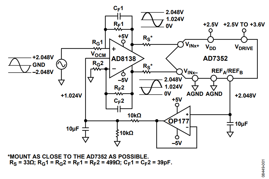
The circuit described in this document provides a dc-coupled, single-ended to differential conversion of a bipolar input signal to the AD7352 dual, 3 MSPS, 12-bit successive approximation register (SAR) analog-to-digital converter (ADC). This circuit is designed to ensure maximum performance of the AD7352 by providing adequate settling time and low impedance.
Circuit Description
For differential operation, simultaneously drive the VINx+ and VINx− pins (x refers to the VINA± and VINB± pins of the AD7352) of the ADC with two equal signals that are 180° out of phase and are centered around the proper common-mode voltage. Because not all applications have a signal preconditioned for differential operation, there is often a need to perform a single-ended to differential conversion. An ideal method of applying differential drive to the AD7352 is to use a differential amplifier, such as the AD8138. This device can be used as a single-ended to differential amplifier or as a differential to differential amplifier. The AD8138 also provides common-mode level shifting. Figure 1 shows how the AD8138 can be used as a single-ended to differential amplifier in a dc-coupled application. The positive and negative outputs of the AD8138 are connected to the respective inputs on the ADC through a pair of series resistors to minimize the loading effects of the switched capacitor inputs of the ADC. The architecture of the AD8138 results in outputs that are highly balanced over a wide frequency range without requiring tightly matched external components. The single-ended to differential gain of the circuit in Figure 1 is equal to the feedback resistor divided by the gain resistor (RF/RG), where RF = RF1 = RF2 and RG = RG1 = RG2.

(Simplified Schematic; Decoupling and All Connections Not Shown)
If the source of the analog inputs being used has zero impedance, all four resistors (RG1, RG2, RF1, and RF2) are the same as shown in Figure 1. If the source has a 50 Ω impedance and a 50 Ω termination, for example, increase the value of RG2 by 25 Ω to balance this parallel impedance on the input and ensure that the positive and negative analog inputs have the same gain. This impedance match also requires a small increase in RF1 and RF2 to compensate for the gain loss caused by increasing RG1 and RG2. For analysis of the terminated source condition, use the ADI DiffAmpCalc interactive design tool and see the MT-076 Tutorial.
The AD7352 requires a driver that has a fast settling time due to the short acquisition time required to achieve 3 MSPS throughput with a serial interface. The track-and-hold amplifier (THA) on the front end of the AD7352 enters track mode on the rising edge of the 13th SCLK period during a conversion. The ADC driver must settle before the THA returns to hold (68 ns later for 3 MSPS throughput on the AD7352 using a 48 MHz SCLK). The AD8138 has a specified 16 ns settling time that satisfies this requirement.
The voltage applied to the VOCM pin of the AD8138 sets up the common-mode voltage. In Figure 1, VOCM is connected to 1.024 V, which is a divided version of the internal 2.048 V reference on the AD7352. If the on-chip 2.048 V reference on the AD7352 is to be used elsewhere in a system (as shown in Figure 1), the output from the REFA or REFB pin must first be buffered. The OP177 features a high op amp and is an ideal choice for a reference buffer.
The AD8138 operates on dual 5 V supplies, where the AD7352 is specified for power supply voltages of 2.5 V to 3.6 V. Ensure that the input maximum input voltage limits of the AD7352 are not exceeded during transient or power-on conditions (see the MT-036 Tutorial). The circuit must be constructed on a multilayer printed circuit board (PCB) with a large area ground plane. Proper layout, grounding, and decoupling techniques must be used to achieve optimum performance (see the MT-031 Tutorial, MT-101 Tutorial, and the EVAL-AD7352 evaluation board layout).
Common Variations
The OP07D, an ultralow offset voltage op amp, is a lower cost alternative to the OP177. It offers similar performance with the exception of the offset voltage specification. Alternatively, the AD8628 or the AD8638 offers very high precision with very low drift with time and temperature.
References
MT-036 Tutorial, Op Amp Output Phase-Reversal and Input Over-Voltage Protection, Analog Devices.
MT-074 Tutorial, Differential Drivers for Precision ADCs, Analog Devices.
MT-075 Tutorial, Differential Drivers for High Speed ADCs Overview, Analog Devices.
MT-076 Tutorial, Differential Driver Analysis, Analog Devices.