AN-1454: Troubleshooting Power Supply with the ADP1074, ADP1071-1, and ADP1071-2: Common Scenarios
Introduction
The ADP1074, ADP1071-1, and ADP1071-2 are isolated, fixed frequency, current mode controllers. The ADP1074 supports synchronous, active clamp forward topologies and ADP1071-1 and ADP1071-2 support synchronous flyback topologies for isolated power supply designs. The proprietary iCoupler® technology by Analog Devices, Inc., is integrated in these controllers, eliminating the bulky signal transformers and optocouplers that transmit signals over the isolation boundary in traditional power supply designs. This technology reduces system design complexity, cost, and component count, and improves overall system reliability. With the integrated isolators and MOSFET drivers on the primary and the secondary sides, the ADP1074, ADP1071-1, and ADP1071-2 offer a compact, system level design that yields higher efficiency than nonsynchronous converters at heavy loads.
The feedback signal and timing of synchronous rectifier pulse width modulators (PWMs) are transmitted between the primary to secondary sides or secondary to primary sides through the iCouplers using a proprietary transmission scheme.
The ADP1074, ADP1071-1, and ADP1071-2 also offer input current protection, undervoltage lockout (UVLO), precision enable with adjustable hysteresis, and overtemperature protection (OTP) features.
This application note describes some of the typical debugging scenarios that the user can encounter when designing a power supply using the ADP1074, ADP1071-1, and ADP1071-2 devices.
Power Supply Related Issues
Power Supply Does Not Start Up
With EN = 0, and VIN > UVLO = 4.5 V, the RT pin measures 1.22 V. If it does not, the RT pin to AGND1 connection is broken.
When the enable pin (EN) is high, the PWM signals (NGATE for ADP1074 and GATE for ADP1071-1 and ADP1071-2) outputs a PWM signal.
When using the ADP1071-1, ensure that the VREG1 pin is powered and reaches 8 V to 12 V typical but is greater than the UVLO voltage of 4.5 V.
Power Supply Keeps Turning On and Off
Identify if the period between retries is around 40 ms or 200 ms. If the former, there is a primary overcurrent protection (OCP) fault. If the latter, the secondary side (VDD2), powered up but lost power at some point in time.
Power Supply Makes an Audible Noise
The following describes several potential issues that can cause the power supply to make an audible noise:
- A mechanical vibration present on the board indicates that the most likely sources of the noise are film capacitors (if any) or the transformer.
- A hissing sound is an indication that the PWMs are not
steady.
- It is advisable to check the system stability to ensure that there is enough phase margin in the control loop design.
- Identify whether there is excessive jitter on the falling edge of the PWMs. The sensing of the primary current signal must be done differentially using the CS and AGND1 pins that are Kelvin connected to the sense resistor.
- The overvoltage protection (OVP) feature in the ADP1074, ADP1071-1, and ADP1071-2 disables the PWMs until the voltage on the OVP pin crosses below the hysteresis level (typically 36 mV). The response to an OVP fault is not shut down and retry; this can cause a hissing sound.
The Power Supply Cannot Be Loaded to Full Load
To troubleshoot the inability to load the power supply to full load, take the following steps:
- Ensure that the sense resistor is sized properly.
- Check the maximum flux density calculations to determine whether the transformer is not saturating.
- Check if the DMAX limit (ADP1074 only) is set properly to prevent maximum duty cycle.
- Check the hiccup timer if it is 40 ms (OCP) or 200 ms (OVP hiccup or VDD2 UVLO hiccup).
Power Supply Regulation and Voltage Droop
If the power supply does not regulate at the proper voltage or the voltage droops by 100 mV to 200 mV when a load is applied, take the following steps to troubleshoot the issue:
- Verify that the output voltage resistor divider is connected and installed properly and set to the correct value.
- Ensure that there is no short or external circuit connection loading the SS2 pin. In steady state, the SS2 pin voltage must be 1.4 V.
- Measure the voltage from FB to AGND2 at the pins of the ADP1074, ADP1071-1, or ADP1071-2 rather than at the output terminals. The voltage is 1.2 V in steady state.
- In the ADP1074, it is recommended that the FB and AGND2 pins are used to differentially sense the output voltage. If using the ADP1071-1 or ADP1071-2 devices, AGND2 needs to be a solid connection and the FB pin needs to be Kelvin connected to the positive output terminal.
Setting the Power Supply to Track a Signal Prior to Soft Start Completion
It is possible for the power supply to track a signal prior to soft start completion by feeding the tracking signal into the SS2 pin. However, when the secondary side wakes up, there can be a small momentary offset before the ADP1074, ADP1071-1, or ADP1071-2 is able to track the signal. This is essentially dependent on the loop bandwidth of the entire system.
Power Supply Enters a 200 ms Hiccup Timer
A power supply entering a 200 ms hiccup timer is caused by a VREG2 UVLO condition or sustained OVP for more than 200 μs. Ensure that there is not an excessive current draw from the VREG2 pin causing the internal regulator to enter current limit.
Regulating to an Output Voltage of Less Than or Equal to 1.2 V
To achieve this sort of regulation requires the use of an auxiliary winding on the secondary side that generates about 6 V to 10 V connected to VDD2; this powers the secondary side of the ADP1074, ADP1071-1, and ADP1071-2 devices.
The output voltage can be sensed directly by feeding the output voltage into the FB pin.
For voltages <1.2 V, such as 1.0 V, use the SS2 pin to adjust the reference. To avoid sudden glitches during the soft start process, it is advisable to turn on this setpoint reference when the SS2 voltage reaches the setpoint voltage during the closed-loop soft start process. Note that the system (such as the transformer turns ratio) is designed so that the duty cycle does not run into minimum on time issues.
Preventing Damage to the Device When Connecting Primary Voltage to VIN and Output Voltage to VDD2
The maximum voltage on VIN to AGND1 and VDD2 to AGND2 is 60 V. The ADP1074, ADP1071-1, and ADP1071-2 devices are rated for continuous operation at this voltage. However, it is recommended to feed in a smaller voltage to reduce dropout losses due to the internal, low dropout (LDO) regulator from VIN to VREG1 and VDD2 to VREG2.
Alternately, to avoid the LDO losses, design auxiliary windings on the transformer so that these windings supply VREG1 and VREG2.
Slope Issues
The Soft Start Ramp Has a Dual Slope
This is normal behavior. The initial portion of the soft start ramp is governed by the SS1 capacitor for the ADP1074 device or the resistor on the GATE pin for the ADP1071-1/ADP1071-2 devices.
The latter portion of the soft start ramp is governed by the SS2 capacitor. In addition, because the devices are current mode controllers, the two slopes cannot be made equal to each other for all load conditions. However, a monotonic soft start ramp is guaranteed for as long as the initial soft start ramp exceeds the latter soft start ramp.
Achieve a Single Slope for the Output Voltage During Soft Start
It is possible to achieve a single slope for the output voltage during a soft start, but it must be at a specific input voltage and output load condition because there are many variables that determine the rate of climb of the output voltage.
Determining Enough Slope Compensation
Use the following formula to set the slope compensation resistor:

where:
RRAMP is the slope compensation resistor.
k = 0.5 (nominal) or 1 (deadbeat control).
VOUT is the output voltage.
L is the output inductor for active clamp forward topology.
L = LPRIMARY/(N1/N2)2 for flyback topology.
N is the turns ratio.
RSENSE is the sense resistor at the CS pin.
TS is the switching period.
Load Issues
Erratic and Choppy Soft Start Ramp
An excessive load can cause the OCP/feedback recovery feature to initiate, causing an erratic and choppy soft start ramp.
The ADP1074, ADP1071-1, or ADP1071-2 Becomes Hot Even at Light Load
The primary and secondary side supply rails, (VDD1 and VDD2, respectively) have a built in LDO to power internal circuitry. VREG1 and VREG2 have nominal voltages of 8 V and 5 V, respectively. The power loss in the ADP1074, ADP1071-1, and ADP1071-2 devices is largely dependent on the loss in the LDOs and the switching frequency because the internal gate drivers on both the primary and secondary sides switch at this rate. A lower drop on the LDOs ensures a lower power dissipation in the device.

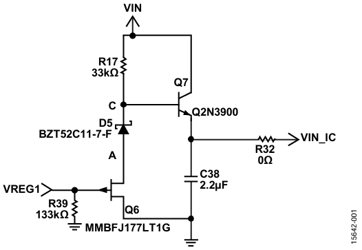
Figure 1. Input voltage for VDD1 with lowest dissipation; VREG1 is powered by auxiliary winding (not shown); zener dissipation is eliminated.

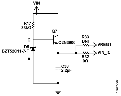
Figure 2. Input voltage for VDD1 with low to medium dissipation; VREG1 is powered by auxiliary winding (not shown).
It is useful to enter light load mode using the MODE pin because it disables the synchronous rectifier (SR) PWMs and enters pulse skip mode when the load is further reduced.
In addition, the voltage on VREG1 must be limited to <14 V because there is an internal 14 V Zener that sinks in current when the voltage is exceeded, causing the ADP1074, ADP1071-1, or ADP1071-2 to become hotter.
Recovery from Shorted Load Sometimes Causes Overshoot
Overshoot sometimes occurs because VDD2 or VREG2 is not yet established and SS2 has not yet been able to catch up with the FB pin voltage. To correct this condition, use a larger SS1 capacitor and a smaller SS2 capacitor.
Difficulty Setting the Light Load Mode Threshold (ADP1074 Only)
Use the MODE pin to set up a light load mode.

where:
RMODE is the MODE pin resistor.
IPEAK_LLM is the peak primary current at the light load condition.
CSGAIN = 12.5.
IMODE is the current flowing out of the MODE pin.
Alternately, using the empirical method involves measuring the COMP pin voltage (VCOMP) at the light load condition and selecting RMODE using the equation
RMODE = VCOMP/6.5 µA
Parallel MOSFETs and High Voltage (>5 V) SRs
The added capacitive load invariably slows down the rise time of the gate source voltage of the MOSFET. The ADP1074, ADP1071-1, and ADP1071-2 have 1 A integrated drivers on the primary and secondary sides. If additional drive strength is required, provide an external buffer, such as a totem pole circuit powered from a dedicated supply, or, alternatively, use an external MOSFET driver. Use this same approach to drive the SRs at a higher voltage.
Signal Issues
SR1 Signal Turns On Before NGATE
It is not a concern if the SR1 signal turns on before NGATE because in the active clamp forward topology, during the freewheeling period, when the primary drain voltage VDS < VIN, the SR1 body diode conducts, thereby causing the secondary winding to short because SR2 was already on. This causes the VDS to be flat at a voltage of VIN (there can be a small resonance ringing between the drain source capacitance of the primary MOSFET (CDS) and the leakage inductance of the transformer, LLEAKAGE). Due to this phenomenon, SR1 can be turned on before NGATE without any repercussions.
Transmitting the Feedback Signal (COMP) to the Primary Side
The COMP signal is transmitted to the primary side using the patented iCoupler technology by Analog Devices.
The Transient Response is Too Slow or the Settling Time is Large
It is recommended to use the ADP1074, ADP1071-1, or ADP1071-2 SIMPLIS model to perform a simulation to provide a bode plot. Typically, in this case, there is an indication of too much phase margin. Decreasing the compensation capacitor at the COMP pin is recommended.
RT Pin Resistance Does Not Measure the Value Soldered on the PCB
When the RT pin resistance does not measure the value that was soldered on the printed circuit board (PCB), it does not mean that the RT pin is damaged. The internal circuity of the device prevents the user from measuring the external resistance on the RT pin. Provided that the RT pin is not open or shorted to ground, this is acceptable.
Delay from OVP Threshold Crossing to PWM Termination
The delay from the OVP threshold crossing to PWM termination is <600 ns.
Soft Start and Soft Stop Problems
Output Voltage Overshoots
The ramp of the primary side soft start must be slower than the secondary side soft start. To do this, increase the SS1 capacitor (ADP1074) or increase the GATE resistor (ADP1071-1 and ADP1071-2). This ramp determines the current limit during the soft start ramp before the secondary side has powered up. If the current limit is too small, the output voltage can rise too fast before the proper handover procedure can take place, that is, control transferring successfully to the secondary side.
Ensuring that the Secondary Side Controls the Power Supply for the Majority of the Soft Start
A resistor capacitor diode (RCD) snubber from the switch node on the secondary side can rectify the switch node voltage on a capacitor, and when fed into the VDD2 pin, enables the secondary side from the start. Control then transfers to the secondary side within the first few switching periods. However, because the switch node can ring excessively high, the power dissipation in the secondary side LDO (VDD2 to VREG2) must be taken into account (see Figure 3).

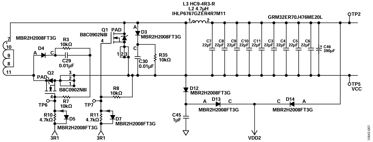
Figure 3. RCD on, switch node powering VDD2.
Ensuring a Smooth Soft Start with a Precharged Output
The ADP1074, ADP1071-1, and ADP1071-2 devices have an SR soft start feature where the SR edges gradually increase from the minimum to the nominal duty cycle at a speed of approximately 1.5 ns/tS, where tS is the switching period. This feature prevents any reverse currents and glitches in the output. In addition, because the device is both a primary and secondary side con troller, the output voltage is always monitored by the secondary side, and the SS2 pin tracks the FB pin (and the output voltage) instantaneously, thereby resulting in zero glitches during startup.
Soft Stop Seems to Toggle Between Stop and Start When Toggling the EN Pin
When toggling the EN pin, if the soft stop appears to be starting, stopping, and starting again, check for any glitches (or narrow voltage spikes) on the EN pin. For example, in Figure 4, the system enters soft stop, then enters normal mode, and then reenters soft stop, but ultimately shuts off after a 100 ms time period. The bounce of a mechanical switch can be a cause of this phenomenon, forcing high frequency voltage spikes on the EN pin that go above and below the EN pin threshold, causing glitches in soft stop.

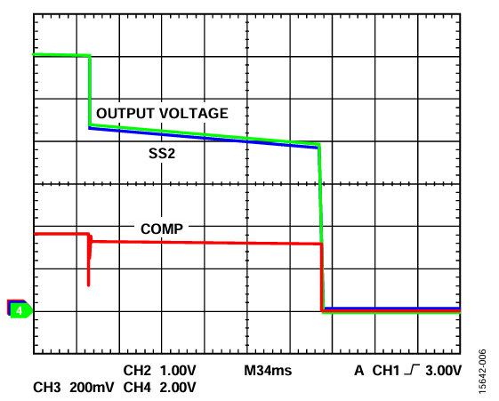
Figure 4. Abnormal soft stop caused by glitch on the enable pin; red trace = COMP, green trace = output voltage, and blue trace = SS2.
Frequency
Maximum Frequency Range
The maximum programmable frequency using the RT pin is 600 kHz. However, using the SYNC pin, the frequency can be increased to 1 MHz.
Frequency Dither for the Supply
The dither function can be added to the SYNC pin by an external source. The SYNC pin synchronizes to the external frequency.
Loss of Output Tracking When Feeding a 0.2 V p-p, 100 kHz Sine Wave at SS2
For tracking, the crossover frequency of the loop gain should be much greater than the input signal at SS2.
Incorrect Synchronization
The synchronization frequency present on the SYNC pin needs to be within ±10% of the frequency set using the RT pin. It takes the ADP1074, ADP1071-1, and ADP1071-2 devices about 10 cycles of the external clock signal before the synchronization feature can lock on and synchronize to the external frequency. Also, ensure that the VIH level of the input signal is high enough.
Typical iCoupler Bandwidth
The typical iCoupler bandwidth is 1.6 MHz.
Current
OCP Recovery Feature Defined
During steady state, the FB pin is at 1.20 V. At this time, the SS2 pin voltage is at 1.4 V. Under abnormal situations, such as an overload condition, the output voltage can dip severely. In such an event, the current limit is at the maximum level and the COMP pin voltage is at its clamp level. If the two conditions of the COMP pin voltage being clamped and the FB voltage, VFB < (1.2 V – 100 mV), occur, the controller discharges the SS2 pin using a fast current sink to make the SS2 pin equal to the FB pin. The controller then attempts to perform a soft start from this precharged condition, that is, from the last known value of the output voltage; this is the OCP/feedback recovery feature.
However, at any time, if the voltage on the COMP pin is above the maximum clamp voltage for more than a period greater than 1.5 ms, the system enters hiccup mode.
During the soft start from precharge, the output voltage rises at the same rate as determined by the capacitor on the SS2 pin. The SS2 pin voltage determines the current limit during this period. If, however, there is a detrimental fault in the power stage that prevents the rise of the output voltage, VFB does not track SS2, and when SS2 > (VFB + 100 mV), the COMP pin voltage increases to the clamp level and the system reenters the OCP/feedback recovery mode.
Typical IDD Consumptions for the Primary and Secondary Sides
Figure 5 and Figure 6 provide current consumption perfor mance data for both the primary and secondary sides, respectively.

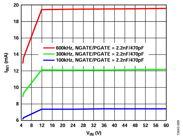
Figure 5. IINI1 current vs. VIN voltage.

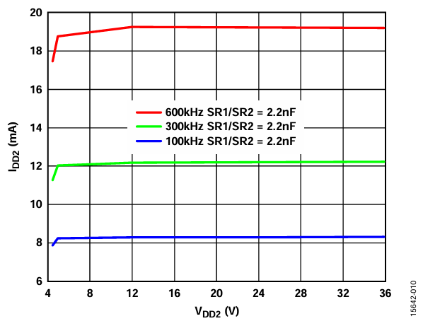
Figure 6. IDD2 current vs. VDD2 voltage.
Proper Method of Sensing the Primary Current Using the CS and AGND1 Pins
The primary current is sensed typically by using a sense resistor in series with the primary switch. Use the CS and AGND1 pins as differential pins. In extremely noisy environments, a small capacitor from 33 pF to 100 pF can be added in close proximity to the CS and AGND1 pins (see Figure 7).

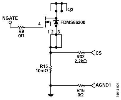
Figure 7. Kelvin sensing of CS signal.

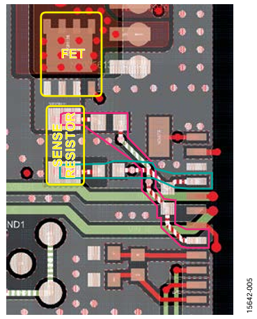
Figure 8. Layout highlighting CS lines in light pink and blue.
Ensuring that Power Consumption from the Drivers Does Not Exceed the Limit of the VREG1 and VREG2 Pins
Use the following formula to determine the current draw from the VREGx pins:

yields:

where:
VREGx is the voltage at the VREG1 or VREG2 pin.
IREGx is the current draw from the VREGX pin.
CGS is the gate source capacitance of the MOSFET.
fS is the switching frequency.
Phase Loss When Transmitting COMP from Secondary to Primary Side
Due to the sampling nature of the output of the error amplifier (COMP pin), the system can be likened to a discrete time system although there are no quantization effects in this system.
However, due to finite encoding time and finite modulation, demodulation time, and propagation delay, it is essential to understand the phase loss that occurs in the system. In the system, the total digital delay is the sum of the encoding, modu lation, and demodulation quantities. The dominant term is the propagation delay of the microtransformer, which is 600 ns, contributing to a phase loss of −600 ns × 20 kHz × 360 = −4.32° for a bandwidth of 20 kHz. The negative sign indicates a phase loss.
Due to the constant sampling process of the current limit (COMP pin voltage), the system is updated with a new level of current limit several times during the switching period. This takes the system several steps above the conventional double update rate (or dual-edge modulation in the analog domain). At a typical switching frequency of 300 kHz, the error amplifier output voltage is sampled 32 times per switching period. For a bandwidth of 20 kHz, this reduces the phase loss to
(1/300k)/32 × 20 kHz × 360 = 0.75°
Decreasing the Variability in the OCP Threshold Over the Line Voltage (ADP1074 Only)
Note that the input rms current is directly proportional to the input voltage and to the output load multiplied by the transformer winding ratio. The ADP1074 does not sense the input rms current, and the current limit is set by sensing the input peak current. The peak inductor output current and the peak input current are correlated by the transformer winding ratio. Therefore, the input peak current limit changes little over the entire input voltage range and is accurate enough for most applications.
The following equations show a detailed analysis of the relationship between input peak current limit and the output inductor current ripple:
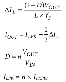
where:
ΔIL is the output inductor current ripple.
D is the duty cycle.
L is the inductance of the output inductor.
IOUT is the output load current.
ILPK is the peak output inductor current at maximum IOUT.
n is the transformer winding turn ratio, N1/N2.
IPKPRI is the peak input current at maximum IOUT.
Figure 9 shows the primary current and secondary current waveforms in continuous conduction mode (CCM), where the primary current is always discontinuous and the secondary is always continuous. The primary current ripple and the secondary inductor current ripple are correlated by the transformer winding turn ratio.

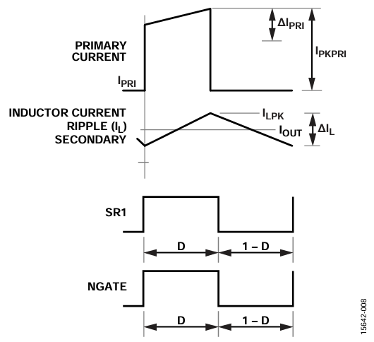
Figure 9. Primary and secondary current waveforms in an active clamp forward topology.
Because IPKPRI is fixed at any input voltage due to the fixed VCSLIM threshold, and because the duty cycle varies at different input voltages, the output current also varies slightly at different input voltages when the input peak current, IPKPRI, crosses over VCSLIM. The difference of the output currents at minimum and maximum input voltages is related by:

where:
ΔIOUTLIMIT s the variation in the output current limit.
IOUTDMIN is the output current limit at the minimum duty cycle, DMIN.
IOUTDMAX is the output current limit at the maximum duty cycle,
DMAX.
ILPK_DMIN is the inductor peak current at DMIN.
ILPK_DMAX is the inductor peak current at DMAX.
ΔIL_DMIN is the inductor current ripple at DMIN.
ΔIL_DMAX is the inductor current ripple at DMAX.
ILPK_DMIN and ILPK_DMAX have the same value because the current limit threshold is fixed over the line voltage. Another way to think of this is that the current limit is the same due to the in built feedforward effect seen in a peak current mode controller.
Therefore, it can be shown that:

From Equation 1, the difference in the output currents at the minimum and maximum input voltages when the input peak current that reaches the VCSLIM threshold is proportional to the difference of DMAX and DMIN, and can be minimized by increasing L and/or fSW. With the proper selection of L and fSW, the output current limit varies little over a large VIN range.
Relationship Between the Maximum and Minimum Available Current Over the Line Voltage for Flyback Converters
The input voltage affects the input peak current, which is at its highest at the minimum input voltage and lowest at the maximum input voltage. Although the input peak current-limit threshold, VCSLIM, is fixed at different input voltages, the output current can vary considerably.
See the following equations for a detailed analysis of the relationship between input peak current limit and the output current.
Given that:

where:
P is the output power.
LP is the primary inductance.
IP is the peak current.
n is the ratio of primary turns to secondary turns of the
transformer.
VO is the output voltage.
VIN is the input voltage.
The difference in power is calculated as:

where:
δP is the variation in output power.
PMAX is the maximum power.
PMIN is the minimum power.
VIN_MIN is the minimum input voltage.
VIN_MAX is the maximum input voltage.
Therefore, this relationship is nonlinear. It is advisable to keep the switching frequency high enough to accept a reasonable switching loss and reduce the range of the input voltage.
Author
