AN-1213: Powering the AD9788 800 MSPS TxDAC Digital-to-Analog Converter Using the ADP2105 Synchronous Step-Down DC-to-DC Regulator for Increased Efficiency
Circuit Function and Benefits
This circuit utilizes a pair of ADP2105 synchronous step-down dc-to-dc regulators to provide the individual power supply rails required for the AD9788 dual channel, 16-bit, high dynamic range TxDAC® digital-to-analog converter. The ADP2105 pair powers the AD9788 at greater than 85% efficiency, which is up to 50% higher than that obtained using a traditional linear regulator solution. Total circuit power dissipation using linear regulators is 1.4 W and using switching regulators only 0.88 W
This increased efficiency results in lower system level power consumption, with no measurable degradation in the performance of the AD9788. The ADP2105 is low noise step-down dc-to-dc converter that uses a fixed frequency, peak current mode architecture with an integrated high-side switch and low-side synchronous rectifier. The high 1.2 MHz switching frequency allows the use of small external inductors and ceramic capacitors; and the tiny 16-lead, 4 mm × 4 mm LFCSP_VQ package minimizes PCB area.
The AD9788 supports DAC update rates to 800 MSPS. The low noise and excellent linearity of the AD9788 enable transmit architectures from baseband to complex IF frequencies up to 200 MHz. The AD9788 features a rich set of digital signal processing, including 2×, 4×, and 8× interpolation filter options and complex digital modulation with a 32-bit NCO resolution, as well as gain, phase, and offset compensation. The DAC outputs interface seamlessly with analog quadrature modulators, such as the ADL537x family.
Circuit Description
| Product | Description |
| AD9788 | Dual, 16-Bit, 800 MSPS TxDAC® digital-to-analog converter with low power 32-bit complex NCO |
| ADP2105 | 1 A, synchronous, step-down DC-to-DC converter |
Figure 1 shows the ADP2105 power supply solution, which supplies the necessary input power rails to the AD9788 DAC. The AD9788 has four power domains: two that require 3.3 V and two that require 1.8 V. The two domains at 3.3 V are DVDD33, which supplies the I/O circuits, and AVDD33, which supplies the DAC internal switch core. The two domains at 1.8 V are DVDD18, which supplies the digital processing circuitry, and CLKVDD18, which supplies the clock receiver and PLL circuitry. The domains requiring 3.3 V are supplied by a single ADP2105 (3.3 V) device, and the domains requiring 1.8 V are supplied by a single ADP2105 (1.8 V) device.

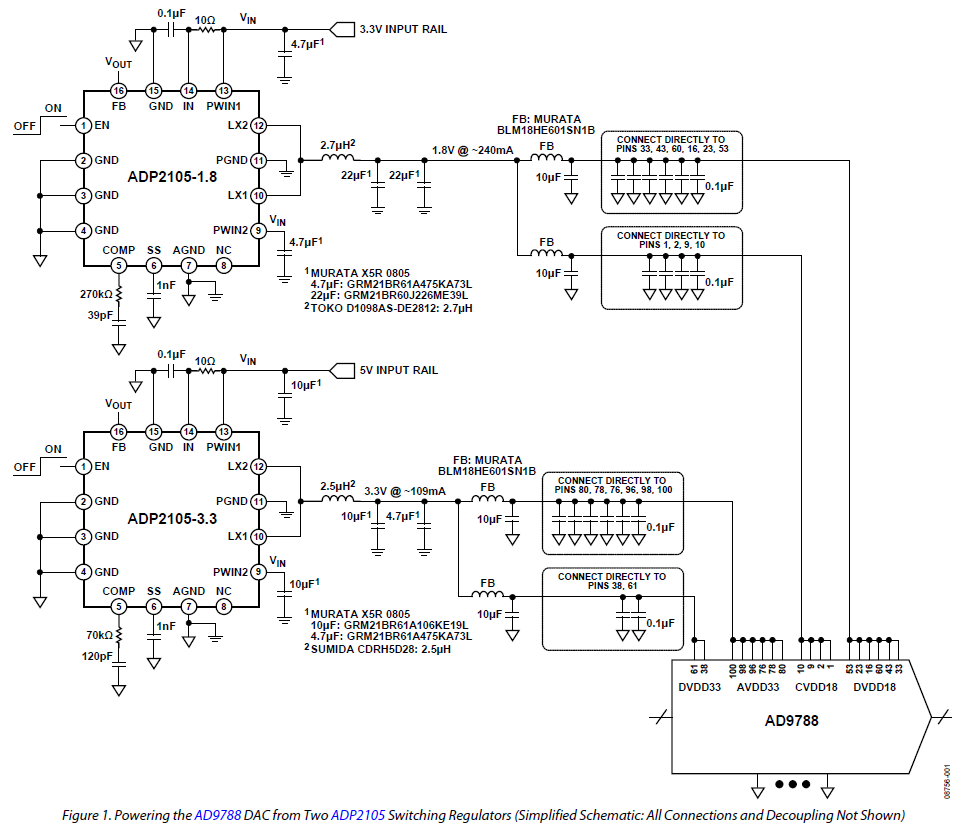
Figure 1. Powering the AD9788 DAC from Two ADP2105 Switching Regulators (Simplified Schematic: All Connections and Decoupling Not Shown).
The power domains of each rail are isolated from each other by use of a ferrite bead, as shown in Figure 1. One bulk capacitor per domain, plus localized high frequency decoupling capacitors on individual supply pins, provide adequate bypassing to preserve the dynamic performance of the AD9788. The input voltage to the ADP2105 impacts the size of the required inductor and also affects the efficiency of the regulator. Lower input voltages generally require smaller inductors and improve the power supply efficiency. The configuration shown uses a 3.3 V input rail to supply the 1.8 V regulator and a 5.0 V input rail to supply the 3.3 V regulator.
Figure 2 shows a representative comparison of the spectral plots from the AD9788 when powered from linear regulators versus the ADP2105 switching regulators. The particular instance shown is for DAC output frequency, FOUT = 125 MHz, DAC input data rate, FDATA = 200 MHz, and 4× interpolation. Under these conditions, the DAC outputs a 125 MHz signal at an 800 MSPS update rate. The output spectrum of the AD9788 shows no measurable increase in noise floor or spurs associated with the switching frequency under the test cases considered.
The efficiency results in Table 1 compare the overall efficiency of an LDO regulator design to the ADP2105 based switching regulator design. The linear regulators and the switching regulators used the same input voltages. The 1.8 V regulators were supplied with 3.3 V input rails. The 3.3 V regulators were supplied with 5.0 V input rails. The use of switching regulators resulted in power savings of 457 mW and an efficiency gain in overall power consumption of about 50%.
Proper component placement, power and ground plane layout, and signal routing are critical to a successful design when using a dc-to-dc regulator, such as the ADP2105. Adhering to the detailed layout guidelines in the switching regulator data sheet should lead to a successful application of the device. These guidelines usually call for switching inductors to be mounted far away from the DAC and sensitive components in the DAC’s clock and signal paths—or on the opposite side of the PCB to help eliminate magnetic flux coupling into sensitive components. High current loops should be kept as short as possible. Bypass capacitors and compensation networks for the regulators should be placed close to the device.
Common Variations
For systems that do not require the full dynamic range of the 16-bit AD9788, the AD9785 and AD9787 offer 12-bit and 14-bit resolution, respectively, with the same feature set and sample rates. The lower resolution devices can also be powered by the ADP2105 without suffering any performance penalty compared to linear regulators, while realizing similar efficiency gains. The ADP2105 supplies a maximum of 1 A output current. For multichannel applications where higher output currents are required, the ADP2106 offers 1.5 A output current, and the ADP2107 offers 2 A output current.
With care, both linear voltage regulators and switching regulators can provide clean power supplies that allow optimal performance from high dynamic range DACs. Linear regulators provide low noise voltage outputs but deliver power inefficiently. Switching solutions show increased efficiency and lower power dissipation without degradation of DAC performance.

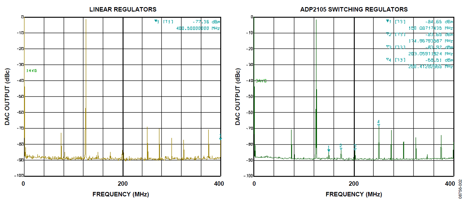
Figure 2. Output Spectrum for DAC Output Frequency = 125 MHz, DAC Input Data Rate = 200 MHz, DAC Output Rate = 800 MSPS (4× Interpolation).
| AD9788 Power Supply Domain Current (mA) | Linear Regulator | ADP2105 Switching Regulator | |||
| Power (mW) | Efficiency (%) | Power (mW) | Efficiency (%) | ||
| DVDD18 + CVDD18 | 240 | 792 | 54 | 475 | 91 |
| DVDD33 + AVDD33 | 109 | 545 | 66 | 405 | 89 |
| Total | 1337 | 59 | 880 | 90 | |
Learn More
Cobb, Michael. Powering High-Speed Analog-to-Digital Converters with Switching Power Supplies. Technical Paper. May 2009.
ADIsimPower™ Regulator Interactive Design Tool