Objective
The circuit we are evaluating in this activity generates an approximate sine wave from a triangle wave by using the properties of the differential pair of transistors contained in the SSM2212 NPN matched transistor pair. We know that the transconductance of a differential pair of transistors is defined as:

Where IO is the differential pair tail current, VIN is the differential input voltage, and VT is the thermal voltage, which is about 26 mV at room temperature.
Materials
- ADALM2000 Active Learning Module
- Solderless breadboard
- Jumper wires
- One 10 kΩ resistor
- Four 4.7 kΩ resistors
- One 2.2 kΩ resistor
- Two 220 Ω resistors
- One 390 Ω resistor
- One 500 Ω potentiometer
- One 100 pF capacitor
- Two small signal NPN transistors (SSM2212 NPN matched pair)
- One operational amplifier (OP27)
Description
Construct the circuit in Figure 1 on your solderless breadboard. The +5 V (Pin 7) and –5 V (Pin 4) power supply connections for the OP27 amplifier are not pictured in the schematic, but remember to connect them or the circuit will not function.


Set the W1 to the following:
- Amplitude (peak-to-peak) = 3.6 V
- Offset = 0 V
- Frequency = 1 kHz
- Triangle wave
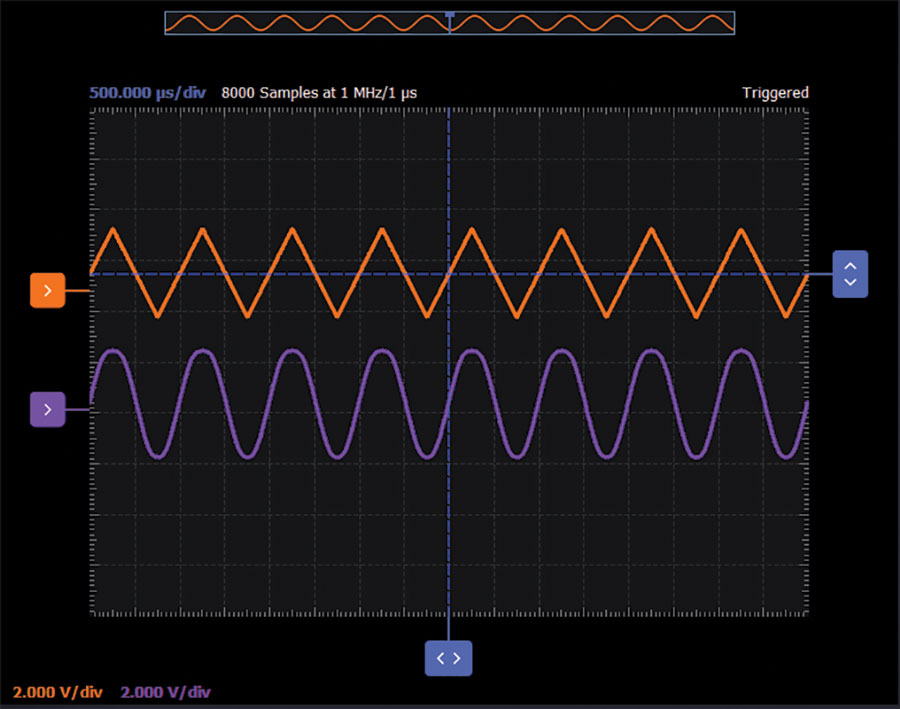
Adjust the 500 Ω potentiometer, R6, for the best symmetry in the output sine wave shape. Using the FFT display and looking for the minimum even order distortion may be a good way to test the quality of the output sine wave. You may want to adjust the amplitude and DC offset of the input triangle wave to see if that can improve the odd order harmonics in the output.
In the case of this circuit, the output voltage will be approximately:

Where RL represents the 4.7 kΩ load resistors on the output. The division by 2 happens because we only take a single-ended output, not a differential output.
So, the output voltage will be a function of the input voltage and the hyperbolic tangent. The first few terms of the Taylor series of the sine and hyperbolic tangent functions are as follows in Equation 3 and Equation 4.


Sine:

Hyperbolic tangent:

Comparing the two Taylor series will show that they both have first-order linearity. What this means is that if we apply a triangle wave to a differential pair with a hyperbolic tangent transfer function and keep the amplitude low—that is, on the order of 2VT—the output should be nearly indistinguishable from a sine wave. The purpose of the 2.2 kΩ and 220 Ω resistors at the input of the differential pair (base of Q1) is to attenuate the triangle wave signal from the AWG to operate the circuit in the range where the output is as low a distortion sine wave as possible.
Hardware Setup
Connect the circuit shown in Figure 1 to a breadboard.
Procedure
Configure the oscilloscope instrument to capture several periods of the two signals being measured. A plot example using Scopy is presented in Figure 3.

Triangle Wave Generator
To make a standalone sine wave generator, we need to replace the ADALM2000 module waveform generator with a triangle wave generator. The AD654 voltage-to-frequency converter IC will be the basis of the triangle wave generator. The normal output of the AD654 is an open collector digital square wave signal. The internal timing circuit of the AD654, however, uses a ramp generator. This internal ramp waveform is available in differential form across the external timing capacitor connected to pins 6 and 7 in Figure 4. We cannot use this triangle wave signal directly without disturbing the internal timing of the AD654. We can use the AD8226 instrumentation amplifier to buffer and convert the differential signal to a single-ended signal. By adjusting the amplitude of this triangle wave signal, we can use it to drive the triangle wave to the sine wave converter circuit from Figure 1.
Materials
- Two 1 kΩ resistors
- One 47 kΩ resistor
- One 6.8 kΩ resistor
- One 220 Ω resistor
- One 5 kΩ potentiometer
- One 0.1 μF capacitor
- One 1 μF capacitor
- One red LED
- One AD654 voltage-to-frequency converter
- One AD8226 in-amp
- One small signal NPN transistor (2N3904)


When connecting the triangle wave output from the AD8226 to the input of the triangle to sine converter, replace the 2.2 kΩ fixed resistor R1 with a 5 kΩ potentiometer to adjust the signal amplitude for an optimal sine wave shape.
Hardware Setup
Connect the circuit shown in Figure 4 to a breadboard.
Procedure
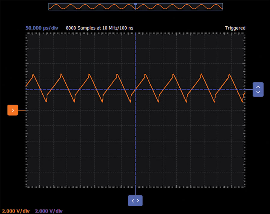
With the use of ADALM2000, the output is shown in Figure 6. We can adjust the gain resistor of the in-amp (R16) so that the output of the circuit will be in the range of the in-amp supply.
In the Scopy plot in Figure 6, R16 is at 168 kΩ.

Question:
- For the circuit in Figure 1, explain how the R6 potentiometer affects the output signal when set to minimum/maximum resistance value.
You can find the answer at the StudentZone blog: ez.analog.com/studentzone.

