Introduction
There are several major advantages to zero-IF architecture. However, there are also some challenges that need to be overcome. Transmit local oscillator leakage (referred to as transmit LOL) is one such challenge. Uncorrected, transmit LOL will produce an unwanted emission within the desired transmission, potentially breaking system specifications. This article discusses the issue of transmit LOL and examines the techniques used to eliminate it, as implemented in ADI’s RadioVerse™ transceiver family (which includes the AD9371; see ADI RadioVerse Website for more details). If transmit LOL can be reduced to a low enough level that it no longer causes system or performance issues, perhaps people can learn to laugh out loud about LOL!
What Is LOL?
An RF mixer has two input ports and one output port, as shown in Figure 1. The ideal mixer would produce an output that is the product of the two inputs. In frequency terms, the output should be FIN + FLO and FIN – FLO, nothing else. If either input is undriven there will be no output.
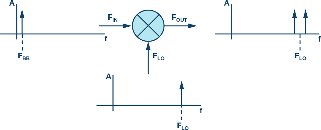
In Figure 1, FIN is set to FBB with a baseband frequency of 1 MHz and FLO is set to FLO with a local oscillator frequency of 500 MHz. If the mixer were ideal it would produce an output that comprises two tones: one at 499 MHz and one at 501 MHz. However, as shown in Figure 2, a real-world mixer will also produce some energy at FBB and FLO. The energy at FBB can be ignored because it is far away from the desired output and will be filtered out by the RF components located after the mixer output. Regardless of the energy at FBB, the energy at FLO can be a problem. It is very close to or within the desired output signal and difficult or impossible to remove by filtering, since the filtering would also filter the desired signal. It is this unwanted energy at FLO that is referred to as LOL. The local oscillator (LO), which drives the mixer, has leaked to the mixer’s output port. There are also other paths for the LO to leak to the system output, such as through power supplies or across the silicon itself. Regardless of how the LO leaks out, it can be referred to as LOL.
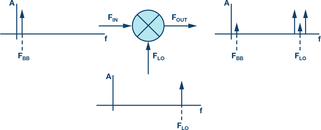
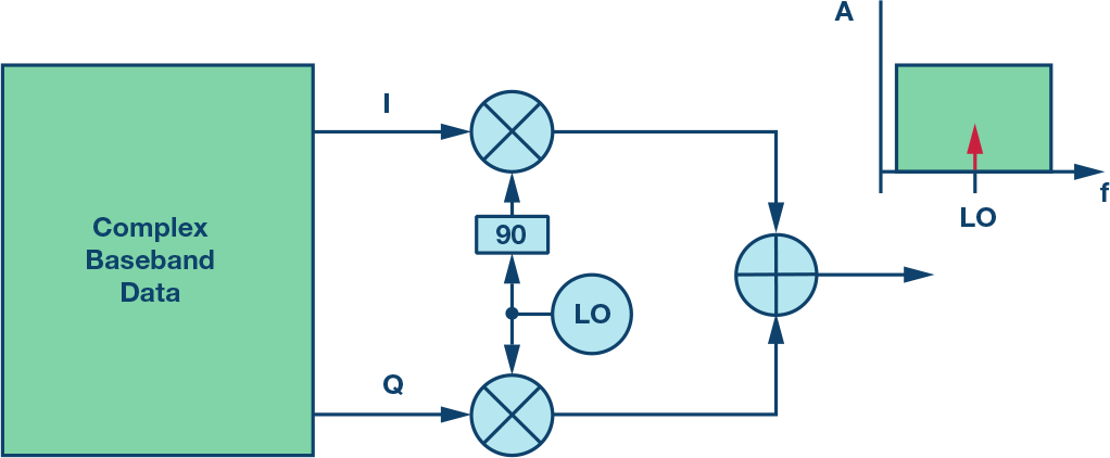
In a real-IF architecture where only one sideband is to be transmitted, it is possible to resolve LOL by using RF filtering. In contrast, in a zero-IF architecture where both sidebands are to be transmitted, the LOL sits in the middle of the desired output and presents a more difficult challenge (see Figure 3). Conventional filtering is no longer an option, because any filtering that would remove the LOL would also remove portions of the wanted transmission. Therefore, other techniques must be used to eliminate it. Otherwise, it will likely end up becoming an unwanted emission within the overall desired transmission.
Eliminating LO Leakage (also Called LOL Correction)
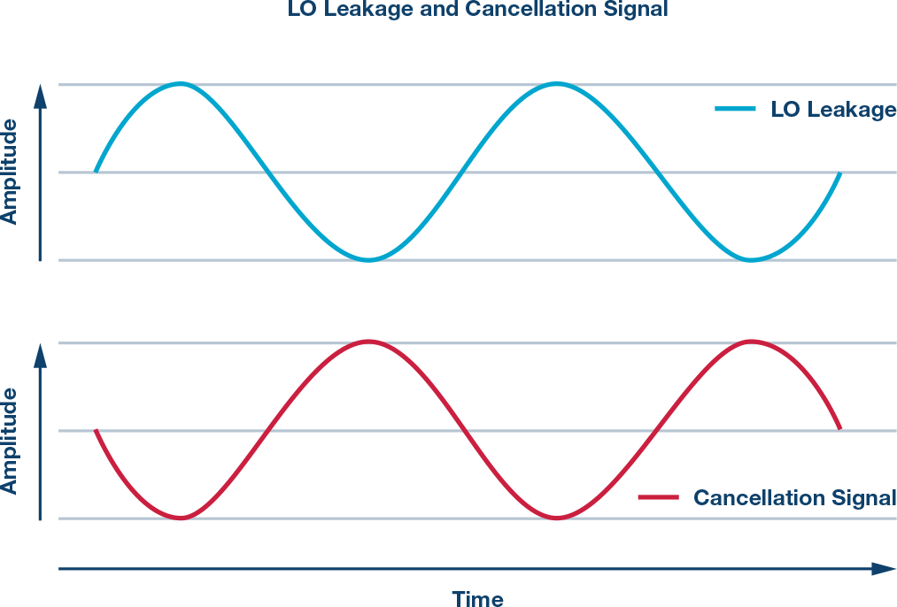
The elimination of LOL is achieved by generating a signal that is equal in amplitude but opposite in phase to the LOL, thus cancelling it, as shown in Figure 4. Assuming we know the exact amplitude and phase of the LOL, the cancellation signal can be generated by applying dc offsets to the transmitter’s inputs.
Generation of the Cancellation Signal
The complex mixer architecture lends itself well to the generation of the cancellation signal. Because quadrature signals at the LO frequency exist in the mixer (they are at the heart of how the complex mixer works),1 they allow for the generation of a signal at the LO frequency with any phase and amplitude.
The quadrature signals that drive the complex mixer can be described as Sin(LO) and Cos(LO)—these are orthogonal signals at the LO frequency that drive the two mixers. To generate the cancellation signal, these orthogonal signals are added together with different weights. In mathematical terms, we can produce an output that is I × Sin(LO) + Q × Cos(LO). By applying different signed values in place of I and Q, the resulting sum will be at the LO frequency and can have any desired amplitude and phase. Examples are shown in Figure 5.

The desired transmission signal will need to be applied to the transmitter’s inputs. By applying a dc bias to the transmission data, the output of the mixer will contain both the desired transmission signal and also the desired LOL cancellation signal. The intentionally generated cancellation signal will combine with the unwanted LOL and they will cancel, leaving only the desired transmission signal.
Observing the Transmit LOL
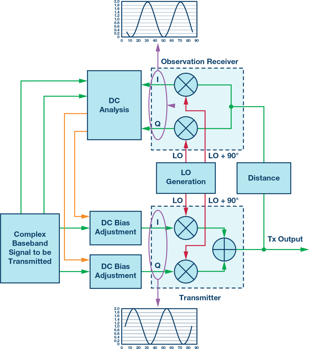
The transmit LOL is observed using an observation receiver, as shown in Figure 6. In this example, the observation receiver uses the same LO as the transmitter, so any transmit energy at the LO frequency will appear as dc at the output of the observation receiver.
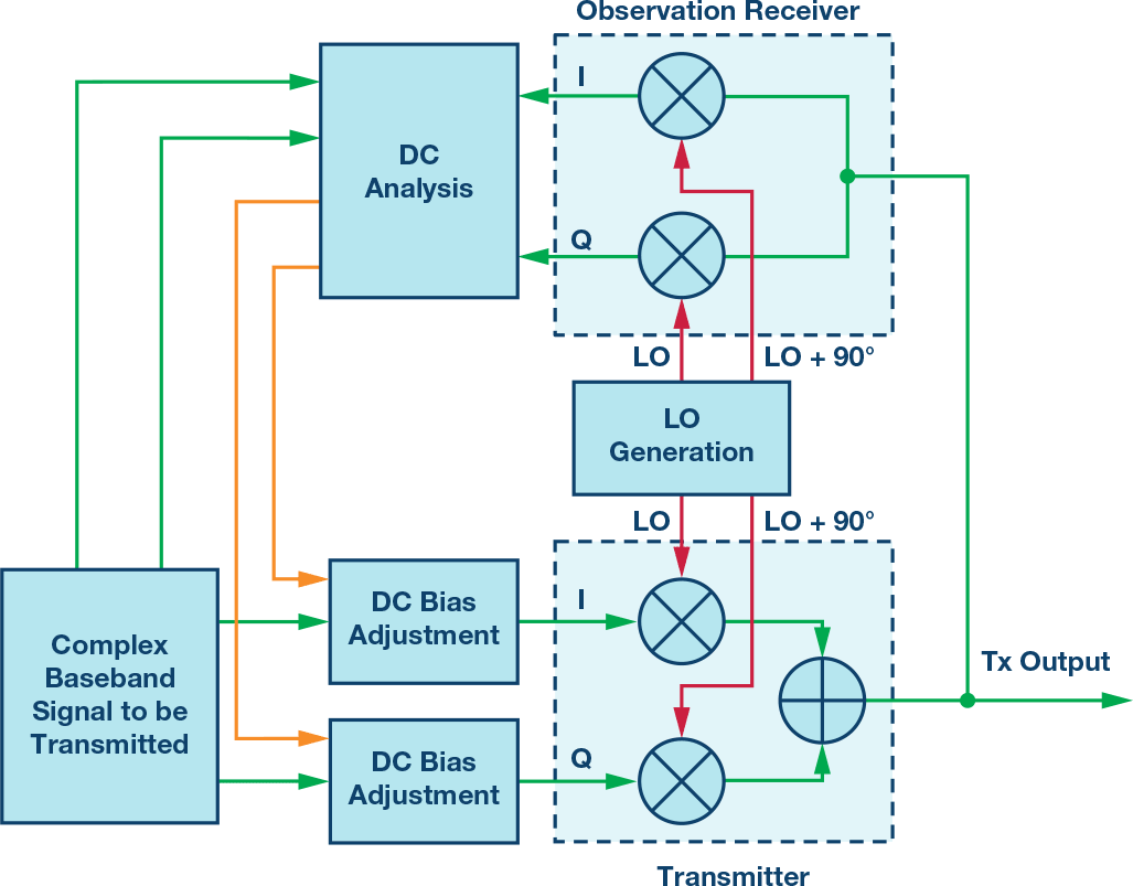
The approach shown in Figure 6 has an inherent weakness: by using the same LO to transmit and observe, transmit LOL will appear as dc in the observation receiver’s output. The observation receiver itself will have some amount of dc due to component mismatch in the circuit, so the total dc output by the observation receiver will be the sum of the transmit LOL and the native dc offset that exists in the observation receiver. There are ways to overcome this issue, but a better approach is to use a different LO frequency for observation, thereby separating the native dc in the observation path from the transmit LOL observation result. This is shown in Figure 7 below.
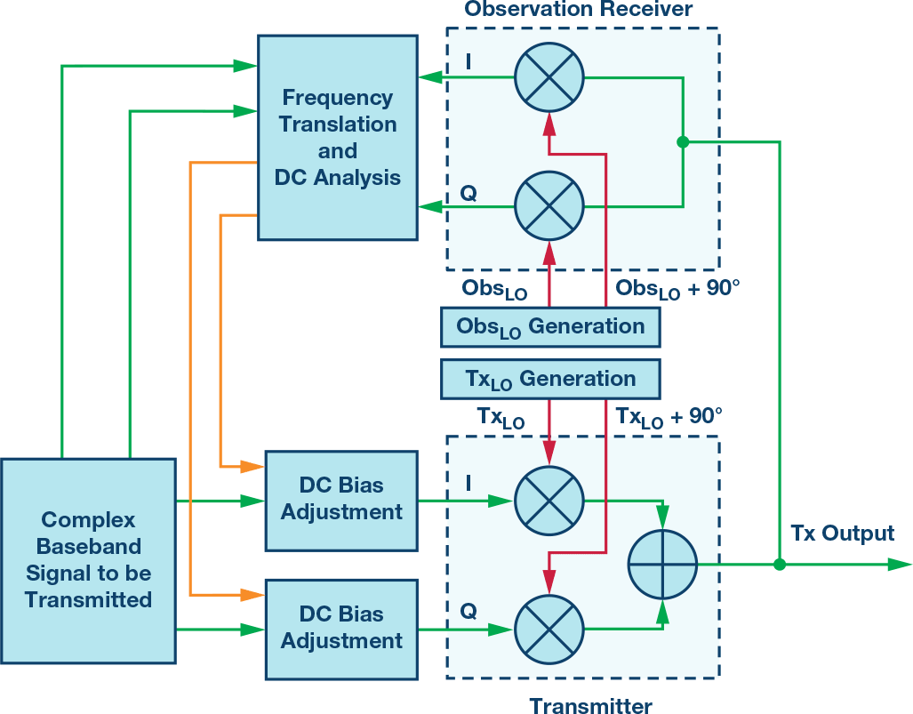
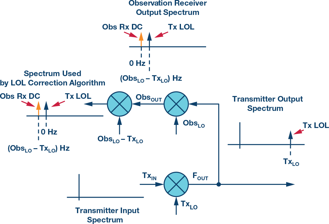
Because the transmission is being observed using a frequency other than transmit LO, energy at the transmit LO frequency will not appear at dc in the observation receiver. Instead, it will appear as a baseband tone whose frequency is equal to the difference between the transmit LO and the observation LO. DC native in the observation path will still appear at dc, so there will be total separation of observation dc and transmit LOL measurement results. Figure 8 illustrates this concept using single-mixer architecture for simplicity. The input to the transmitter is zero in this example, so the only output from the transmitter is transmit LOL. Frequency shifting is done after the observation receiver to move the transmit LOL observed energy to dc.
Finding the Necessary Correction Values
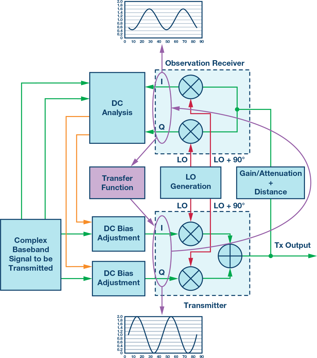
The required correction values are found by taking the observation receiver’s output, dividing it by the transfer function from transmit input to observation receiver output, and comparing this result to the intended transmission. The transfer function in question is shown in Figure 9.
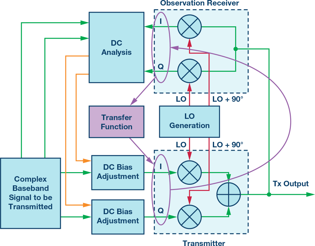
The transfer function from the transmitter baseband input to the observation receiver baseband output is comprised of two components: amplitude scaling and phase rotation. Each is explained independently in more detail in the following sections.
Figure 10 shows that the amplitude of the transmit signal reported by the observation receiver may not represent the actual amplitude of the transmit signal being transmitted if the loopback path from transmit output to observation receiver input has gain or attenuation in the path, or if the gain of the transmitter circuit were different from the gain of the observation receiver circuit.

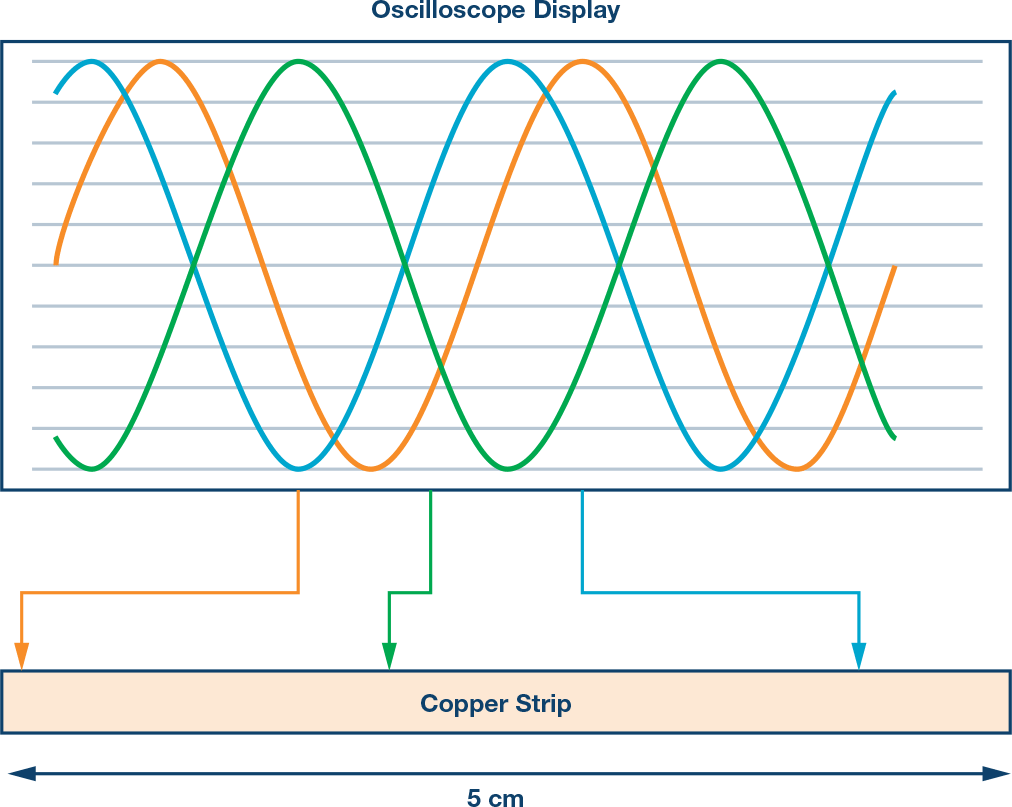
Now let’s consider phase rotation. It is important to realize that signals do not travel instantaneously from point A to point B. For example, signals travel through copper at approximately half the speed of light, meaning that a 3 GHz signal travelling along a copper strip has a wavelength of approximately 5 cm. This means that if the copper strip is probed with multiple oscilloscope probes spaced a few centimeters apart, the oscilloscope will show multiple signals that are out of phase with each other. Figure 11 illustrates this principle, showing three scope probes that are spaced out along a copper strip. The signal seen at each point is at a frequency of 3 GHz, but there is a phase difference between the three signals.
Note that moving a single scope probe down the copper strip would not show this effect, as the scope would always trigger at 0° phase. It is only by using multiple probes that the relationship between distance and phase can be observed.
Just as there is a phase change along the copper strip, there will be a phase change from transmitter input to observation receiver output, as shown in Figure 12. It is essential that the LOL correction algorithm knows how much phase rotation has occurred for it to compute the correct correction values.
Determining the Transfer Function from Transmit Input to Observation Receiver Output
The transfer function shown in Figure 13 may be learned by applying an input to the transmitter and comparing it to the output from the observation receiver. However, some points need to be kept in mind. If a static (dc) signal is applied to the transmitter input, it will produce an output at the transmit LO frequency and the transmit LOL will combine with it. This will prevent the transfer function from being learned correctly. It should also be noted that the transmit output may be connected to an antenna, so intentionally applying signals to the transmitter input may not be allowed.
To overcome these challenges, the ADI transceivers use an algorithm that applies a low level dc offset to the transmitted signal. The offset level is adjusted periodically and these perturbations will show up in the observation receiver’s outputs. The algorithm then analyzes the deltas in input values compared to the deltas in observed values, as outlined in Table 1. In this example there is no user signal being transmitted, but the method still holds in the presence of user signal.
| Tx Input Signal | Tx Output Port | Observation Receiver Output | |
| Case 1 | DC offset 1 | TxLO 1 + Tx LOL | (TxLO 1 + Tx LOL) × transfer function |
| Case 2 | DC offset 2 | TxLO 2 + Tx LOL | (TxLO 2 + Tx LOL) × transfer function |
By performing a subtraction of the two cases, the constant transmit LOL is eliminated from the equation and the transfer function can be learned. The number of cases can be expanded to more than two, giving many independent results that can be averaged to increase the accuracy.
Summary
The LOL correction algorithm will learn the transfer function from transmit input to observation receiver output. It will then take the observation receiver’s output and divide it by the transfer function to refer it to the transmitter’s input. By comparing the dc levels in the intended transmission to the dc levels in the observed transmission, the transmit LOL will be determined. Finally, the algorithm will compute the necessary correction values to eliminate the transmit LOL and apply them as a dc bias to the desired transmission data.
This article provides an overview of one aspect of the algorithms used in ADI’s RadioVerse transceivers. For a broader understanding on the concepts of zero-IF and algorithms, see this article on complex RF mixers.1

