Abstract
This article focuses on Type 2 electric vehicle supply equipment (EVSE) design. The rules that must be followed when building an EVSE are found in the IEC 61851-1 standard, and the specific rules for EVSE Type 2 are available in the supplementary standard, IEC 62752. The guidelines follow the standards and are exemplified by the new reference design from Analog Devices. The negotiation between an electric vehicle (EV) and an EVSE during a charging session is presented through the control pilot (CP) waveform, highlighting the states defined in the standard. The waveforms together with the presented debug messages validate the guidelines and offer a better understanding of the EV charging process, thus making the design process easier.
Introduction
The electric vehicle (EV) market is continuously and exponentially growing, and around 500 million EVs are expected to be on the road by 2030. This number seems plausible looking at the data provided by the International Energy Agency1, such as comparing the historical data between 2022 and 2023 with a 35% increase (from 10.2M to 13.8M) in battery electric vehicle (BEV) and plug-in hybrid electric vehicle (PHEV) combined sales. The same agency projects that the world sales in 2030 will reach 40.7M p.a. and 56.5M p.a. in 2035. Issues on climate change and air pollution in highly populated residential areas are the main drivers for high efficiency and zero tail-pipe emission transportation modes.2,3 With the foreseeable growth in the number of EVs, the market not only needs to cope with the demand but also be able to deliver the most efficient charging solutions—covering affordability, safety, and environmental impact.
Lower power charging levels are deemed sufficient since most personal vehicle users drive only around 30 miles per day on average as reported by Solaronev4 for different world regions. The data for the U.S.A. is based on Statista5 and the Federal Highway Administration database6. For home EV charging stations, the in-cable control and protection devices (IC-CPD) supplied with newly purchased EVs are viable solutions since these can eliminate the high costs involved in high power level installation and maintenance. With the current complexity in charging solutions considerations, not only will the EV market grow in the future, but the charging equipment market will as well.
What Is Electric Vehicle Supply Equipment (EVSE) and Where Is It Used?
An EVSE is a device that allows the user to charge a PHEV or BEV safely. EVSEs are classified based on charging power levels. A charging level in EV terminology refers to the electric power distribution type, standards, and maximum power of a charging system as defined by SAE J1772, and internationally adopted under IEC 62196-1.
Mode 2 Standard Functionality
Mode 2 is a method for the connection of an EV to a standard socket-outlet of an AC supply network, utilizing an AC EVSE with a CP function and system for personal protection against electric shock placed between the standard plug and the EV [IEC 62752:2017 6.2.2].
The most important function that is implemented with an IC-CPD is the protection against electric shocks. This is implemented with a residual-current device (RCD), at least type A, and an auxiliary circuit to detect DC currents, or with a type B RCD. This function is crucial because the charger can be used outdoors, in public areas where there is the possibility of contact with water, and where it can be touched by people accidentally or intentionally. The protective earth must be present and, in case of a fault, the supply must be disconnected.
Figure 1 presents a general block schematic of a type 2 IC-CPD. By using a schematic derived from this one, all the mandatory functions in the IEC 61851-1 standard can be implemented. Depending on the preferred solution, some blocks must be added or can be excluded from the general schematic. For example, if the current is sensed through a current transformer, then the isolation IC can be excluded when interfacing with the microcontroller unit (MCU). In the same manner, the weld detection circuit can be excluded if a relay with weld detection is used.


Analog Devices Type 2 EVSE
The block schematic, Figure 2, of the Analog Devices Type 2 EVSE includes the ADE9113 3-channel isolated sigma-delta (Σ-Δ) ADC for voltage and current measurement on the single-phase power input and measurement of the relay voltage for solder contact detection.
Safe operation is enabled by the inclusion of a 6 mA DC/30 mA rms RCD. Detection of overvoltage, undervoltage, overcurrent, overtemperature, protective earth (PE) detection, and EV diode presence is also available. The integrated isolation makes the connection with the MCU straightforward. The MAX32655 ultra low power Arm® Cortex®-M4 processor implements the logic for system control and communication with the EV over the CP interface. The solution also includes a programming and debugging interface. The device’s Bluetooth® 5.2 interface enables connectivity to external devices. The communication between the MCU and the ADE9113 is implemented over SPI.


The CP needed for implementing the communication between the EVSE and EV is generated using the MAX32655 and the ADA4523-1 low noise, zero-drift op amp.
The system is powered by the single phase 230 V AC input. An isolated AC-to-DC switch-mode power supply (SMPS) is used to deliver 12 V to the board and the MAX20457 high efficiency dual synchronous buck converters for automotive applications are used to step down the voltage to 5 V and 3.3 V, providing power to the isolated side of the board. The LT8330 used in the inverting configuration generates the 12 V negative voltage needed for the low side of the CP signal.
The ADT75 12-bit digital temperature sensor monitors the temperature of the device and sends it to the MCU for protection against overheating.
The design is accompanied by an open-source software stack and reference applications, enabling custom software development to start with a proven implementation validated to meet the applicable standards. The system is designed to the IEC 61851 and IEC 62752 standards.
The Isolated ADC
The ADE9113 is an isolated 3-channel sigma-delta ADC for polyphase energy measurement applications using shunt current sensors. Data and power isolation are based on ADI’s iCoupler® technology. This IC features three ADCs. One channel is dedicated to measuring the voltage across a shunt when the shunt is used for current sensing. Up to two additional channels are dedicated to measuring voltages, which are usually sensed using resistor dividers. In this application, one of the voltage channels is used to detect if the relay contacts are soldered.
This ADC includes an isoPower® device, an integrated, isolated DC-to-DC converter. The DC-to-DC converter provides the regulated power required by the first stage of the ADCs. This device eliminates the need for an external DC-to-DC isolation block. The iCoupler chip scale transformer technology is also used to isolate the logic signals between the first and second stages of the ADC. The result is a small form factor, total isolation solutions. It provides access to the ADC outputs, configuration, and status registers for easy interfacing with microcontrollers. It can be clocked from a crystal or an external clock signal.
The pin’s input range of the ADE9113 must be satisfied by choosing the appropriate values for the voltage divider resistors and for the shunt resistance. The range represents the peak-to-peak pseudo differential voltage that must be applied to the ADCs to generate a full-scale response when the IM and VxM pins are connected to AGND, Pin 11. The IM and VxM pins are connected to AGND using antialiasing filters.
Relay Soldered Contact Detection
The second voltage input of the ADE9113 is used for the soldered relay contact detection.
Figure 3 shows the simplified LTspice® simulation for the circuits connected to the three input channels of the ADE9113 where:
R_contact is the value of the relay contact resistance (open, Figure 4, or closed relay, Figure 5, value depending on the simulated case).
V1P, V2P, V1M, V2M, IP, and IM are the inputs of the ADE9113 channels.
The relay state values for the two cases for an input voltage of 230 V amplitude and 23 Ω load are presented in Table 1.


Table 1. ADE Channel Voltages and Current Channel Values for the Opened and Closed Relay Cases
| Relay States | V1P | V2P | IP |
| Opened | 305 mV | 0 mV | 0 mV |
| Closed | 305 mV | 305 mV | 10 mV |
Grid Protective Earth Presence Test
The grid protective earth presence and phase-neutral reversed are sensed during the device power-off using the circuit in Figure 6. If the earth is not present, the device enters an error state and an error message is displayed on the status LEDs. If the phase-neutral reversed needs to be detected, then the two outputs of the optocoupler are used in conjunction with the PE_ERR signal.


Software Framework
no-OS is a software framework by Analog Devices for systems that do not include an operating system (OS), otherwise known as bare metal. This framework defines a common interface (API) for accessing typical bare metal peripherals such as general-purpose input output (GPIO), SPI, I2C, RTC, timer, interrupt controller, and others. This common API may then be used to initialize and control these peripherals in a common way across multiple microcontroller platforms. The framework currently supports Intel and Xilinx microprocessors and SoCs as well as ADI’s own precision microcontrollers, several MAX32xx microcontrollers, STMicroelectronics’ STM32, Raspberry Pi’s PICO, and mbedOS-based devices.
By using this common driver API, which follows its own coding style, no-OS can provide reference projects for ADI evaluation boards running on various underlying hardware. Thanks to the no-OS build system, no-OS users may generate standalone reference projects in a short period of time and use them as the starting point for their own development.
no-OS is an open-source software, and its official repository is the no-OS GitHub repository. Users are free to use and distribute no-OS, provided that they comply with the license. The no-OS main drivers used in the firmware are the ones concerned with the MAX32655 microcontroller, the ADE9113 isolated, 3-channel sigma-delta ADC, and the ADT75 temperature monitoring system.
The State Machine
The functionality of an IC-CPD is presented in Figure 7. The implemented state machine follows the IEC 61851-1 guidelines.
The firmware uses three enums to implement the logic. First is the charger_state_e, which includes the possible states, and the states change based on the CP value. The state_ machine_events_e enum contains all the possible events that can be triggered. These events are used for state logic implementation. The interface_err_status_e enum is used for error interpretation.


Test Results
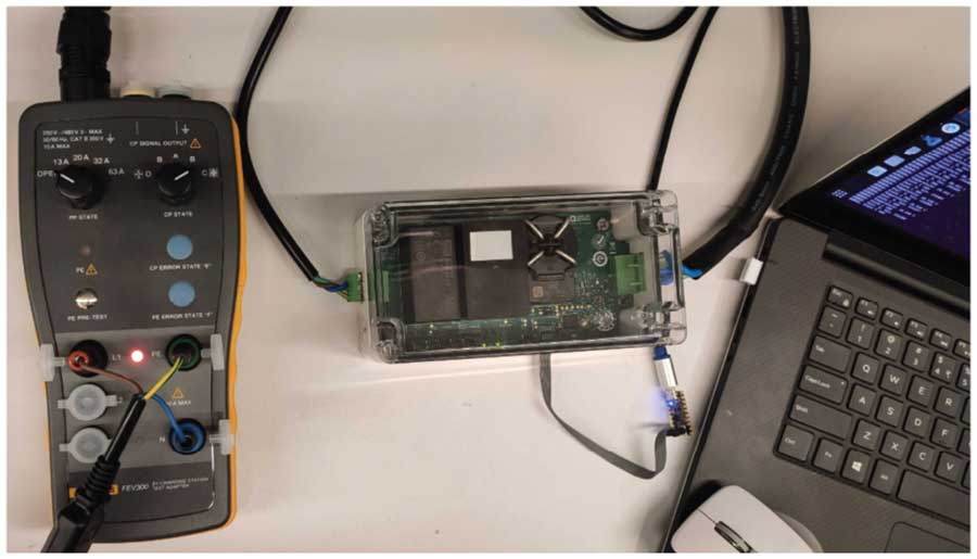
The tests were conducted using the Fluke FEV300 EV charging station adapter and different loads (Figure 8) or with the Type 2 cable connector using the same loads, or an EV.

Normal Working Conditions (Charging State Machine) and RCD Error Detection Results
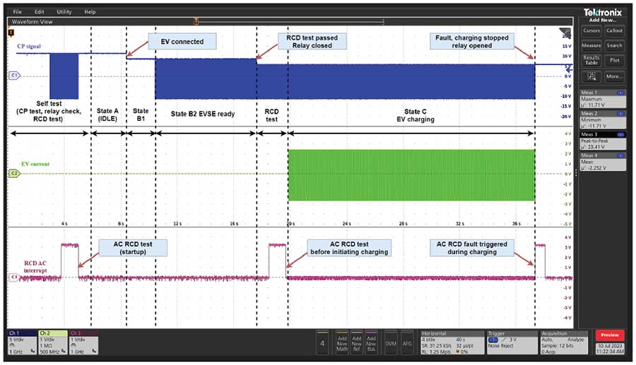
Figure 9 and Figure 10 present the waveforms for two test measurements done using the test bench from Figure 8.
Figure 9 presents a complete run of the state machine from power-up, with the EV disconnected (a resistive load in this case), to charging, where the states are highlighted on the CP waveform.
The difference between Figure 9 and Figure 10 is that during state C (while the EV is charging), an AC RCD interrupt is triggered. This can be observed in the third waveform. The IC-CPD opens the relay, and an error message is displayed on the LEDs.

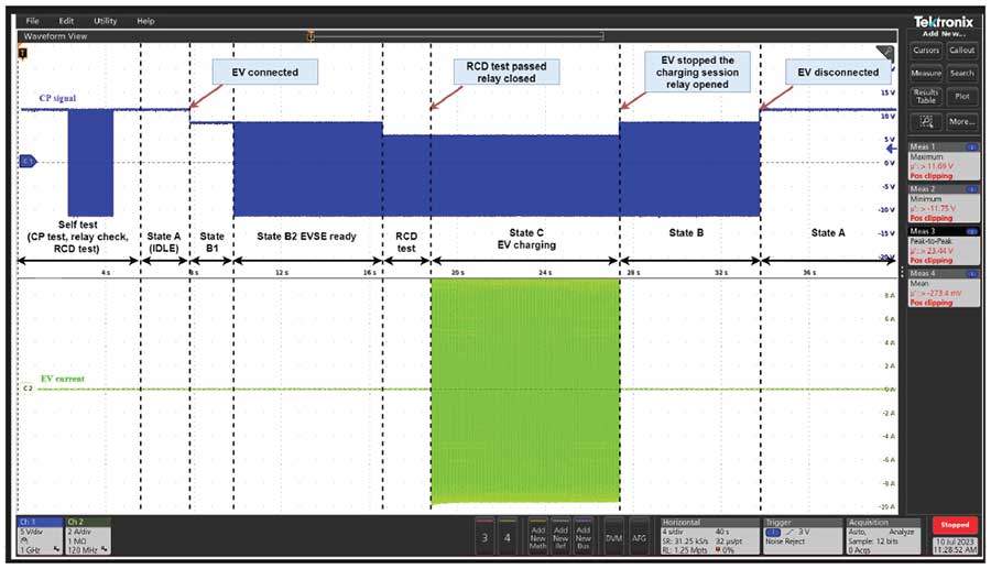

The messages in Figure 11 correspond to the case presented in Figure 9, which shows a complete charging session from power-on to charging and EV disconnected.

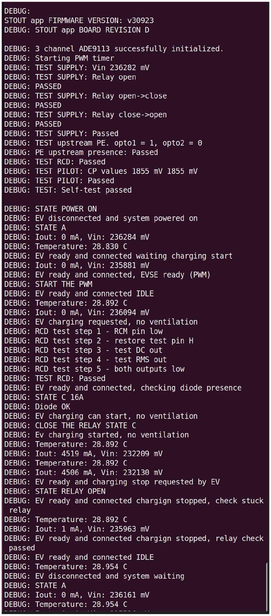
The debug messages also include information about the input voltage value, the current and temperature inside the enclosure, and the active states at a specific moment in time.
CP Error
In case of a CP error, the IC-CPD opens the relay and indicates the CP error on the LEDs.
Protective Earth (PE) Error
In case of a PE error (PE missing between EVSE and EV) that occurs in state C, the relay will be opened, and an error will be indicated on the LEDs. If the PE error occurs during state A or state B, the IC-CPD will see it as if the EV is disconnected and will remain or enter state A (depending on the state active when the error occurred). In this situation, the CP level cannot reach the state C value and the relay will remain open until the PE connection is reestablished.
Conclusion
This article is focused on IC-CPDs and offers information about the ADI AD-ACEVSECRDSET-SL reference design, which is a complete Type 2 EVSE 3.6 kW charging cable solution intended for the evaluation and prototyping of EV charging systems. The component count is reduced by using the ADE9113 isolated ADC; this is possible due to its integrated isoPower technology and internal isolation. The MAX32655 MCU with its integrated BLE and ADC channels makes the implementation of the state machine straightforward as indicated in the IEC 61851-1. The use of the no-OS framework and the open-source code approach eases the development of the software and gives a good starting point for the development of software that follows the guidelines in the applicable IEC standards mentioned in the article. The provided flowcharts, debug messages, and the validation of the design with the FEV300 help to better understand and evaluate the whole design.
For further information regarding the reference design, please visit:
- AD-ACEVSECRDSET-SL User Guide
- AD-ACEVSECRDSET-SL Hardware User Guide
- AD-ACEVSECRDSET-SL Software User Guide
References
1 Global EV Data Explorer. International Energy Agency.
2 Fayez Alanazi. “Electric Vehicles: Benefits, Challenges, and Potential Solutions for Widespread Adaptation.” Applied Sciences, Vol. 13, 2023.
3 Luis Sarmiento, Nicole Wägner, and Aleksandar Zaklan. “The Air Quality and Well-Being Effects of Low Emission Zones.” Journal of Public Economics, Vol. 227, 2023.
4 “Worldwide Daily Driving Distance is 25-50km? What about AU, US, UK, EU, and...” Solar on EV, October 2021.
5 “Daily Miles of Travel per Driver in the United States Between 2001 and 2017.” Statista, 2021.
6 National Household Travel Survey. U.S. Department of Transportation Federal Highway Administration.
ADI Type2 EVSE. GitHub.
no-OS API. Analog Devices, Inc.
no-OS Build Guide. GitHub.
no-OS Code Style Guidelines. GitHub.
no-OS GitHub Repository. GitHub.
no-OS Licence. GitHub.
no-OS Overview. Analog Devices, Inc.
