
MAX38913

MAX38913
RECOMMENDED FOR NEW DESIGNS4µVRMS Ultra-Low-Noise 1A LDO with Two-Level Output-Voltage Selection
Industry’s First 1A, 4µV Lowest Output Noise LDO with Smallest Total Solution Size
- Part Models
- 4
- 1ku List Price
- Starting From $1.67
Viewing:
Overview
- Delivers Flexible Output Range
- 1.8V to 5.5V Input Voltage Range
- 0.6V to 5.0V Output Voltage Range
- 1A Maximum Output Current
- 28mV Dropout at 1A Load Current and 5.0V Supply
- 33mV Dropout at 1A Load Current and 3.6V Supply
- Excellent DC and AC Performance
- 1% Regulation over Line, Load, and Temperature
- 4µVRMS of Output Noise, 10Hz to 100kHz
- 75dB PSRR at 10kHz
- High-Level System Integration
- Integrated Pass-Through Function
- Fast Active Discharge of 6Ω at OUT
- Dynamic Two-Level Voltage Scaling with 33 Levels for Each Option for Flexible Configuration (MAX38913)
- 2V, 2.3V Pre-Programmed Voltage Levels (MAX38914)
- Stable with 4µF (Minimum Capacitance)
- Overcurrent and Overtemperature Protection
- Power-OK/Power-on-Reset Output
- Operation Temperature Range from -40°C to +125°C
- Package
- 12-Bump, 0.4mm-Pitch WLP
- 14-Pin, 3mm x 3mm TDFN
The MAX38913/MAX38914 is a low-noise linear regulator that delivers up to 1A of load current with as low as 4μVRMS of output noise. The MAX38913/MAX38914 can dynamically change its output voltage between two separate levels. The MAX38913/MAX38914 has the pass-through mode which, when enabled, completely bypasses the linear regulator.
This regulator maintains ±1% output accuracy over a wide input voltage range, temperature, and load conditions. The no-load quiescent current in the regulation mode is 1.37mA. During the pass-through mode, unlike the conventional dropout mode of an LDO, the MAX38913/MAX38914 consumes very little quiescent current. The MAX38913/MAX38914 has a 6Ω active discharge feature to quickly discharge output capacitors of up to 300μF.
The MAX38913 has 33 programmable output-voltage settings for both voltage selections. The MAX38914 has pre-programmed output voltage levels of 2.3V and 2V. The MAX38913/MAX38914 is packaged in either a space-saving 12-bump WLP or a full-featured 3mm x 3mm, 14-pin TDFN package. Optional power-OK and power-on-reset pins are available in the 14-pin TDFN version.
Applications
- Image Sensors
- Portable Sensor Applications
- SD Memory Cards
Documentation
Data Sheet 1
Brochure 1
ADI has always placed the highest emphasis on delivering products that meet the maximum levels of quality and reliability. We achieve this by incorporating quality and reliability checks in every scope of product and process design, and in the manufacturing process as well. "Zero defects" for shipped products is always our goal. View our quality and reliability program and certifications for more information.
| Part Model | Pin/Package Drawing | Documentation | CAD Symbols, Footprints, and 3D Models |
|---|---|---|---|
| MAX38913AANC+ | WLCSP | ||
| MAX38913AANC+T | WLCSP | ||
| MAX38913AATD+ | 14-Lead TDFN (3mm x 3mm x 0.75mm) | ||
| MAX38913AATD+T | 14-Lead TDFN (3mm x 3mm x 0.75mm) |
This is the most up-to-date revision of the Data Sheet.
Software Resources
Can't find the software or driver you need?
Request a Driver/SoftwareEvaluation Kits
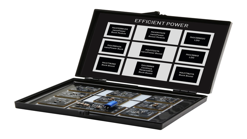
Essential Analog Efficient Power Toolkit for the MAXM38643 / MAX38640 / MAX77839 / MAXM17225 / MAX17227A / MAX38889 / MAX38902C / MAX38913 / MAX77827
Essential Analog Efficient Power Toolkit for the MAXM38643 / MAX38640 / MAX77839 / MAXM17225 / MAX17227A / MAX38889 / MAX38902C / MAX38913 / MAX77827
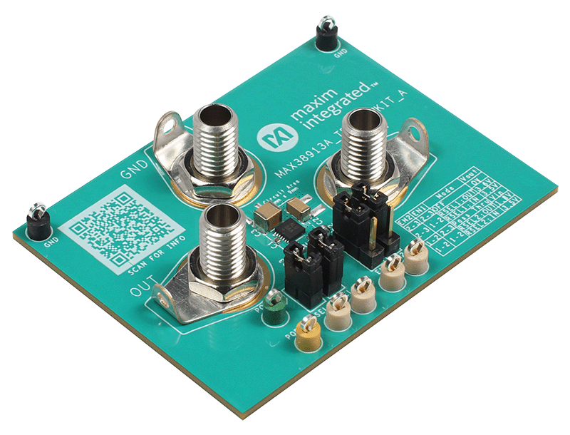
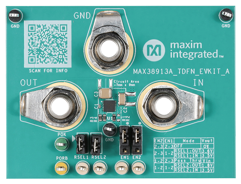
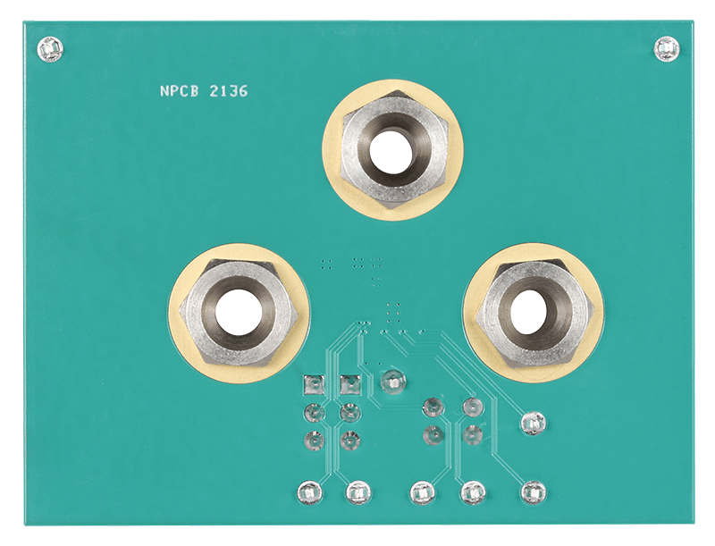
Evaluation Kit for the MAX38913 and MAX38914
Resources
Evaluation Kit for the MAX38913 and MAX38914
Resources
Latest Discussions
No discussions on MAX38913 yet. Have something to say?
Start a Discussion on EngineerZone®