
MAX16166

MAX16166
RECOMMENDED FOR NEW DESIGNSHighly Integrated, 4-Channel Sequencer and Supervisor
Widest Voltage Range Sequencer in Smallest Footprint with Integrated Supervisory
- Part Models
- 2
- 1ku List Price
- Starting From $5.16
Viewing:
Overview
- 2.7V to 16.0V Wide Operating Voltage Range
- Monitor Up to 5 Voltages
- Sequence Up to Four Voltages
- Power-Off in Reverse Order or Simultaneously
- Unlimited Daisy Chain
- Capacitor-Adjustable Sequencing Delay
- Capacitor-Adjustable Power Good Timeout
- Resistor-Configurable Power-Supply On and Off Thresholds
- Open-drain (MAX16165)/Push-pull (MAX16166) Outputs
- POK Output for System Microcontroller Reset
- Bidirectional FAULT Input/Output
- 4x5-Bump WLP and 20L TQFN Package
- -40°C to +125°C Operating Temperature Range
The MAX16165/MAX16166 monitor up to five voltages and sequence up to four voltages. These devices provide an adjustable delay as each supply is turned on as well as monitor each power-supply voltage, including the input voltage VDD.
The MAX16165/MAX16166 operate from a supply range of 2.7V to 16V and have an internal regulator output (ABP), power internal circuits, and supply more than 1mA additional current to any external circuitry.
The sequencing is enabled by two inputs, ON and OFF. A rising edge on the ON input initiates power-on sequencing of the channels whereas a falling edge on OFF input initiates power-off sequencing. During the power-on sequencing, when all of the voltages reach their final values, a sequencing done output DONE asserts high followed by a Power-OK (POK) output after the reset delay timer has expired, allowing the microcontroller (μC) to operate. If any voltage falls below its threshold, the reset output asserts and all voltage supplies are turned off. When the sequencer initiates a power-off sequencing, the MAX16165/MAX16166 can reverse sequence the outputs.
Output options available are open-drain (MAX16165) and push-pull (MAX16166). The MAX16165/MAX16166 can be daisy-chained unlimited amount to time to control any number of voltages in a system.
The MAX16165/MAX16166 feature a bidirectional active low FAULT input/output, which asserts low during any fault condition. FAULT stays low as long as an undervoltage event is present at UVSET Input and it is a one-shot output during all other FAULT conditions. An external signal pulling FAULT low disables all outputs immediately. The MAX16165/MAX16166 are available in a 1.63mm x 2.03mm, 20-bump Wafer-Level Package (WLP) and a 4mm x 4mm, 20L TQFN package. The device is fully specified over the -40°C to +125°C operating temperature range.
Applications
- Latch-Up Prevention and Inrush Current Protection in Multi-Supply Systems
- FPGA/ASIC Power Supply Sequencing
- Servers and Security Cameras
- Test Equipment
- Networking Equipment
- Industrial Sensors and Motor Controls
Documentation
Data Sheet 1
Technical Articles 1
Product Selector Card 1
Product Selection Guide 1
ADI has always placed the highest emphasis on delivering products that meet the maximum levels of quality and reliability. We achieve this by incorporating quality and reliability checks in every scope of product and process design, and in the manufacturing process as well. "Zero defects" for shipped products is always our goal. View our quality and reliability program and certifications for more information.
| Part Model | Pin/Package Drawing | Documentation | CAD Symbols, Footprints, and 3D Models |
|---|---|---|---|
| MAX16166AWPH+ | WLCSP | ||
| MAX16166AWPH+T | WLCSP |
This is the most up-to-date revision of the Data Sheet.
Software Resources
Can't find the software or driver you need?
Request a Driver/SoftwareTools & Simulations
IBIS Model 1
Evaluation Kits
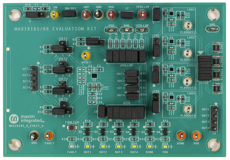
Evaluation Kit for the MAX16165/MAX16166
Evaluation Kit for the MAX16165/MAX16166
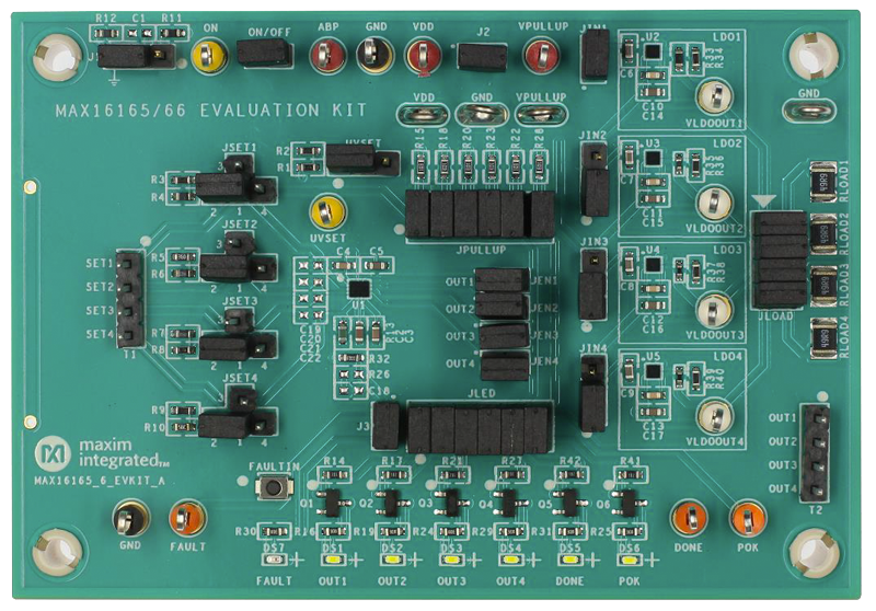
Evaluation Kit for the MAX16165/MAX16166
Evaluation Kit for the MAX16165/MAX16166