ADN4680E
RECOMMENDED FOR NEW DESIGNS250 Mbps, Half Duplex, Quad M-LVDS Transceivers
- Part Models
- 2
- 1ku List Price
- Starting From $3.57
Overview
- Four M-LVDS transceivers (driver and receiver pairs)
- Switching rate: 250 Mbps (125 MHz)
- Independent pin select for each receiver, two modes:
- Type 1: input hysteresis of 15 mV typical
- Type 2: differential input threshold voltage offset by 100 mV to support open-circuit, short-circuit, and bus idle fail-safe
- Compatible with the TIA/EIA-899 standard for M-LVDS
- Glitch free power-up/power-down on the M-LVDS bus
- Controlled transition times on the driver output
- Common-mode range: −1 V to +3.4 V, allowing communication with ±2 V of ground noise
- Driver outputs high-Z when disabled or powered off
- Independent enable pins for each driver and receiver
- Enhanced ESD protection on bus pins
- ≥±15 kV HBM, air discharge
- ≥±8 kV HBM, contact discharge
- ≥±10 kV IEC 61000-4-2, air discharge
- ≥±8 kV IEC 61000-4-2, contact discharge
- Enhanced ±8 kV HBM ESD protection for all pins, contact discharge
- Operating temperature range: −40°C to +105°C
- Available in 48-lead, 7 mm x 7 mm LFCSP
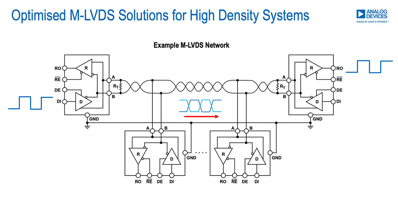
The ADN4680E comprises four multipoint, low voltage differential signaling (M-LVDS) transceivers (driver and receiver pairs) that can operate at up to 125 MHz, or 250 Mbps nonreturn to zero (NRZ). The driver and receiver of each transceiver are connected in half-duplex configuration, which allows each transceiver to be configured via independent enable pins for either sending or receiving data. Electrostatic discharge (ESD) protection of up to ±15 kV is implemented on the bus pins. The transceivers are optimized for low dynamic power consumption for use in high density applications. The ADN4680E is designed to the TIA/EIA-899 standard for use in M-LVDS networks and complement TIA/EIA-644 LVDS devices with additional multipoint capabilities.
The receivers detect the bus state with a differential input of as little as ±50 mV over a common-mode voltage range of −1 V to +3.4 V. Each receiver can be independently pin selectable as a Type 1 or Type 2 receiver. Type 1 receivers have 15 mV of hysteresis so that slow changing signals or loss of input does not lead to output oscillations. Type 2 receivers exhibit an offset threshold, guaranteeing the output state when the inputs are open (open circuit fail-safe), the bus is idle (bus idle or terminated fail-safe), or when the inputs are hard short circuited.
The device is available in a compact 48-lead, 7 mm × 7 mm LFCSP and operates over a temperature range of −40°C to +105°C.
APPLICATIONS
- Backplane and cable multipoint data transmission
- Multipoint clock distribution
- Low power, high speed alternative to shorter RS-485 links
- Networking and wireless base station infrastructure
- Grid infrastructure and relay protection systems
- Differential extension of SPI networks
Documentation
Data Sheet 1
User Guide 1
Application Note 2
Video 2

Webcast 1
ADI has always placed the highest emphasis on delivering products that meet the maximum levels of quality and reliability. We achieve this by incorporating quality and reliability checks in every scope of product and process design, and in the manufacturing process as well. "Zero defects" for shipped products is always our goal. View our quality and reliability program and certifications for more information.
| Part Model | Pin/Package Drawing | Documentation | CAD Symbols, Footprints, and 3D Models |
|---|---|---|---|
| ADN4680EBCPZ | 48-Lead LFCSP (7mm x 7mm w/ EP) | ||
| ADN4680EBCPZ-RL | 48-Lead LFCSP (7mm x 7mm w/ EP) |
This is the most up-to-date revision of the Data Sheet.
Hardware Ecosystem
Tools & Simulations
IBIS Model 1
Evaluation Kits


Evaluating the ADN4680E 250 Mbps, Half-Duplex, Quad M-LVDS Transceivers