

MAX20860A
PRODUCTIONDual-Phase 60A, 16V, Scalable Step-Down Regulator with PMBus and AVSBus
- Part Models
- 2
- 1ku List Price
- Starting From $8.86
Overview
- High Power Density with Low Component Count
- Dual-Phase Operation
- Compact 4.25mm x 10mm, 36-Pin, FC2QFN Package
- Internal Compensation
- Single-Supply Operation with Integrated LDO for Bias Generation
- Wide Operating Range
- Scalable to up to Four-Phase Operation with External Power Stages
- 5V to 16V Input Voltage Range
- 0.4V to 5.8V Output Voltage Range
- 308kHz to 2MHz Configurable SwitchingFrequency
- -40°C to +125°C Junction Temperature Range
- Optimized Performance and Efficiency
- 93% Peak Efficiency with VDDH = 12V and VOUT = 1.2V
- High Efficiency with Optional External Bias InputSupply
- AMS to Improve Load-Transient Response
- Differential Remote Sense
- PMBus and AVSBus Interfaces
- Adaptive Voltage Scaling of 0.4V to 0.8V Reference Range
- PMBus Telemetry of Output Current, OutputVoltage, Input Voltage, and Junction Temperature
The MAX20860A is a fully integrated, highly efficient, dual-phase step-down DC-DC switching regulator with PMBus and AVSBus interfaces. The device operates from 5V to 16V input supplies, and the output can be adjusted from 0.4V to 5.8V, delivering up to 60A of load current. The MAX20860A can work with up to two external power stages delivering up to 120A load current. When the device is configured to dual-phase operation, the minimum input voltage range can be configured to 2.7V using PMBus.
The switching frequency of the device can be configured from 308kHz to 2MHz, to provide the capability of optimizing the design in terms of size and performance.
The MAX20860A utilizes fixed frequency, current-mode control with internal compensation. The IC features selectable advanced modulation scheme (AMS) to provide improved performance during fast load transients. Operation settings and configurable features can be selected by connecting a pin-strap resistor from PGM_ pin to ground or using PMBus commands.
The MAX20860A has internal 1.8V LDO outputs to power the gate drivers (VCC1 and VCC2) and internal circuitry (AVDD and DVDD). The device also has an optional LDO input pin (LDOIN), allowing connection from a 2.5V to 5.5V bias input supply for optimized efficiency.
The IC has multiple protections including positive and negative overcurrent protection, output overvoltage protection, and overtemperature protection to ensure robust design.
The device is available in 4.25mm x 10mm FC2QFN package. It supports -40°C to +125°C junction temperature operation.
Applications
- Data Center Power
- Communications Equipment
- Networking Equipment
- Servers and Storage
- Point-of-Load Voltage Regulators
Documentation
Data Sheet 1
User Guide 2
Product Selector Card 1
ADI has always placed the highest emphasis on delivering products that meet the maximum levels of quality and reliability. We achieve this by incorporating quality and reliability checks in every scope of product and process design, and in the manufacturing process as well. "Zero defects" for shipped products is always our goal. View our quality and reliability program and certifications for more information.
| Part Model | Pin/Package Drawing | Documentation | CAD Symbols, Footprints, and 3D Models |
|---|---|---|---|
| MAX20860AAFX+ | LFCSP | ||
| MAX20860AAFX+T | LFCSP |
| Part Models | Product Lifecycle | PCN |
|---|---|---|
|
Apr 20, 2026 - 2571E PIN/ERRATA |
||
| MAX20860AAFX+T | PRODUCTION | |
This is the most up-to-date revision of the Data Sheet.
Software Resources
Can't find the software or driver you need?
Request a Driver/SoftwareEvaluation Kits
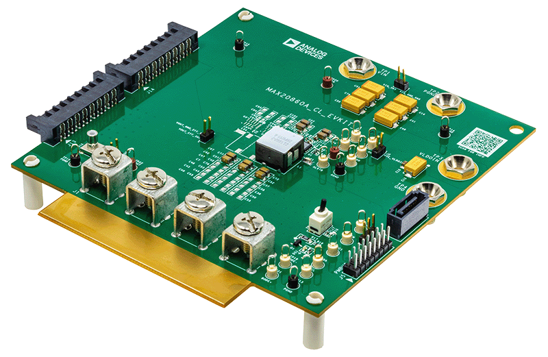
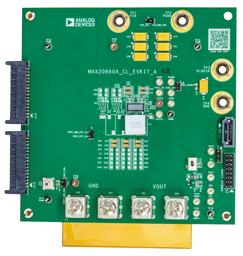
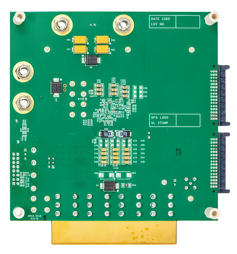
Evaluates: MAX20860A