

MAX17614
RECOMMENDED FOR NEW DESIGNS4.5V to 60V, 3A, Ideal Diode/Power Source Selector with Current Limit, UV, OV Protection
- Part Models
- 2
- 1ku List Price
- Starting From $1.80
Overview
- Ideal Diode Operation
- Fast Reverse Current-Blocking Protection(140ns)
- Seamless Power Source Switchover
- Robust Protection Reduces System Downtime
- Wide Input Supply Range: +4.5V to +60V
- Hot Plug-in Tolerant without transient voltage suppressor (TVS) up to 35V Input Supply
- Negative Input Tolerance to -65V
- Low RON 130mΩ (typ)
- Thermal Shutdown Protection
- Programmable Startup Blanking Time
- Extended -40°C to +125°C Temperature Ranger
- Flexible Design Options Enable Reuse and Less Requalification
- Adjustable Input Undervoltage Lockout (UVLO) and Overvoltage Lockout (OVLO) Thresholds
- Programmable Forward-Current Limit: 0.15A to 0.3A with +3.6% and -3.3% Accuracy and 0.3A to 3A with ±3.3% Accuracy Over Full Temperature Range
- Programmable Current Limit Fault Response: Autoretry, Continuous, and Latch-Off Modes
- Built-in Fault Indication Signals: UVOV and FLAG
- Saves Board Space and Reduces External BOM Count
- 20-Pin, 4mm x 4mm, TQFN-EP Package
- Integrated Back-to-Back nFETs
The MAX17614 ideal diode/power source selector device offers adjustable protection boundaries for systems against positive and negative input faults up to +60V and -65V, and output load current up to 3A. The device features two internal nFETs connected in series with a low cumulative RON of 130mΩ (typ) and can be used to implement an ideal diode function to provide reverse input voltage and reverse current protection with improved system efficiency. Input undervoltage protection can be programmed between 4.5V and 59V, while the overvoltage protection can be independently programmed between 5.5V and 60V. Additionally, the device has an internal default UVLO rising threshold set at 4.2V (typ).
The device is enabled or disabled through the EN pin by a main supervisory system. This in turn offers a switch operation to turn on or turn off power delivery to connected loads.
The current through the device is limited by setting a current limit, which is programmed by a resistor connected from SETI to GND. The current limit can be programmed between 0.15A to 3A. When the device current reaches or exceeds the set current limit, the internal nFET Q2 is controlled to limit the current to set limit. The device offers three current-limit modes: Autoretry, Continuous, and Latch-off. The SETI pin also presents a voltage with reference to GND, which under normal operation is proportional to the device current. The voltage appearing on the SETI pin might be read by an analogto- digital converter or ADC in a monitoring system for recording instantaneous device current.
The device offers FLAG and UVOV communication signals to indicate different operational and fault signals. The communication signal pins are open drain in nature and require external pullup resistors to appropriate system interface voltage.
The device offers internal thermal shutdown protection against excessive power dissipation.
APPLICATIONS
- Small Total Solution Size
- Faster Response Times
- Tight Current Limit Accuracy
Documentation
Data Sheet 1
Video 1

Analog Dialogue 1
ADI has always placed the highest emphasis on delivering products that meet the maximum levels of quality and reliability. We achieve this by incorporating quality and reliability checks in every scope of product and process design, and in the manufacturing process as well. "Zero defects" for shipped products is always our goal. View our quality and reliability program and certifications for more information.
| Part Model | Pin/Package Drawing | Documentation | CAD Symbols, Footprints, and 3D Models |
|---|---|---|---|
| MAX17614ATP+ | Thin Quad Flatpack, No Leads | ||
| MAX17614ATP+T | Thin Quad Flatpack, No Leads |
| Part Models | Product Lifecycle | PCN |
|---|---|---|
|
Apr 20, 2026 - 2571D PIN/ERRATA |
||
| MAX17614ATP+T | PRODUCTION | |
This is the most up-to-date revision of the Data Sheet.
Software Resources
Can't find the software or driver you need?
Request a Driver/SoftwareEvaluation Kits
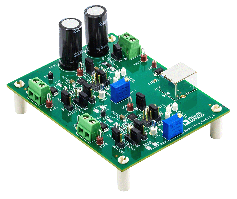
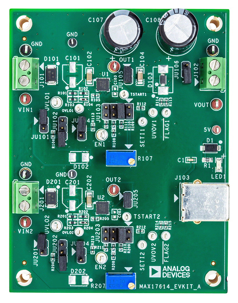
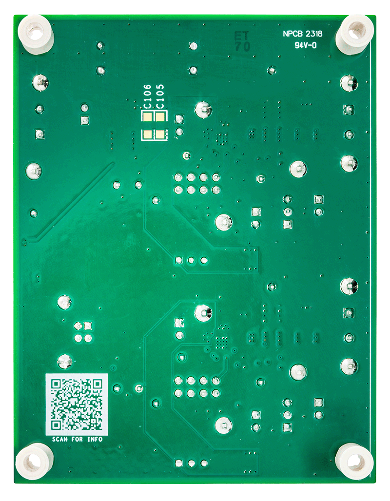
Evaluates: MAX17614 in Ideal Diode/Power Source Selector Applications