

ADP5003
PRODUCTIONLow Noise Micro PMU, 3 A Buck Regulator with 3 A LDO
- Part Models
- 1
- 1ku List Price
- Starting From $3.71
Overview
- Low noise, dc power supply system
- High efficiency buck for first stage conversion
- High PSRR, low noise LDO regulator to remove switching ripple
- Adaptive LDO regulator headroom control option for optimal efficiency and PSRR across full load range
- Precision enable inputs for both the buck regulator and LDO
- 3 A, low noise, buck regulator
- Wide input voltage range: 4.2 V to 15 V
- Programmable output voltage range: 0.6 V to 5.0 V
- 0.3 MHz to 2.5 MHz internal oscillator
- 0.3 MHz to 2.5 MHz SYNC frequency range
- 3 A, low noise, NFET LDO regulator (active filter)
- Wide input voltage range: 0.65 V to 5 V
- Programmable output voltage range: 0.6 V to 3.3 V
- Differential point of load remote sensing
- 3 μV rms output noise (independent of output voltage)
- PSRR > 50 dB (to 100 kHz) with 400 mV headroom at 3 A
- Ultrafast transient response
- Power-good output
- −40°C to +125°C operating junction temperature range
- 32-lead, 5 mm × 5 mm, LFCSP
The ADP5003 integrates a high voltage buck regulator and an ultralow noise low dropout (LDO) regulator in a small, 5 mm × 5 mm, 32-lead LFCSP package to provide highly efficient and quiet regulated supplies
The buck regulator is optimized to operate at high output currents up to 3 A. The LDO is capable of a maximum output current of 3 A and operates efficiently with low headroom voltage while maintaining high power supply rejection.
The ADP5003 can operate in one of two modes. Adaptive mode allows the LDO to operate with an optimized headroom by adjusting the buck output voltage internally in response to the LDO load current. Alternatively, the ADP5003 can operate in independent mode, where both regulators operate separately from each other, and where the output voltages are programmed using resistor dividers.
The LDO regulator output can be accurately controlled at the point of load (POL) using remote sensing that compensates for the printed circuit board (PCB) trace impedance while delivering high output currents.
Each regulator is activated via a dedicated precision enable input. The buck switching frequency can be synchronized to an external signal, or programmed with an external resistor.
Safety features in the ADP5003 include thermal shutdown (TSD), input undervoltage lockout (UVLO) and independent current limits for each regulator. The ADP5003 is rated for a −40°C to +125°C operating junction temperature range.
APPLICATIONS
- Low noise power for high speed analog-to-digital converter (ADC) and digital-to-analog converter (DAC) designs
- Powering RF transceivers and clocking ICs
Documentation
Data Sheet 1
User Guide 1
Technical Articles 1
ADI has always placed the highest emphasis on delivering products that meet the maximum levels of quality and reliability. We achieve this by incorporating quality and reliability checks in every scope of product and process design, and in the manufacturing process as well. "Zero defects" for shipped products is always our goal. View our quality and reliability program and certifications for more information.
| Part Model | Pin/Package Drawing | Documentation | CAD Symbols, Footprints, and 3D Models |
|---|---|---|---|
| ADP5003ACPZ-R7 | 32-Lead LFCSP (5mm x 5mm w/ EP) |
This is the most up-to-date revision of the Data Sheet.
Software Resources
Can't find the software or driver you need?
Request a Driver/SoftwareTools & Simulations
LTspice
Models for the following parts are available in LTspice:
- ADP5003
LTspice® is a powerful, fast and free simulation software, schematic capture and waveform viewer with enhancements and models for improving the simulation of analog circuits.
Evaluation Kits
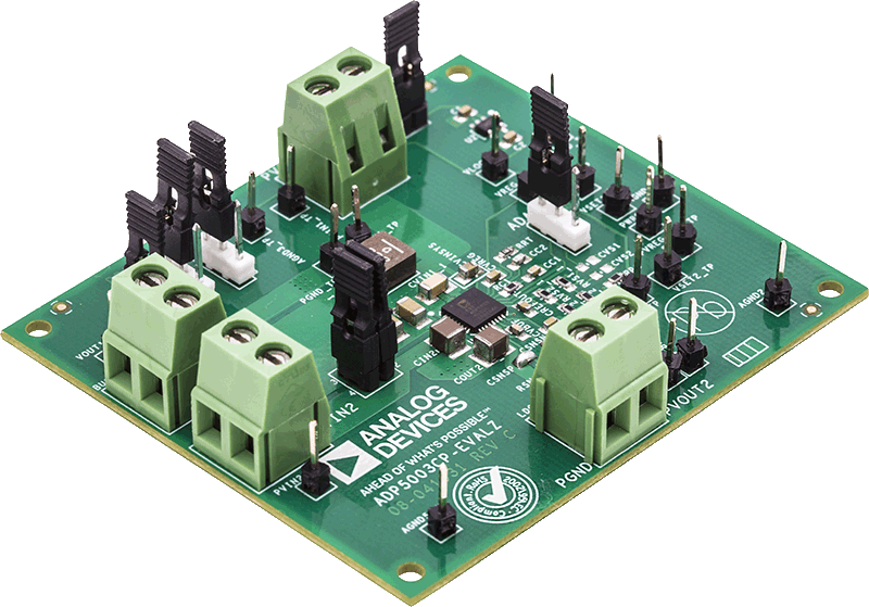
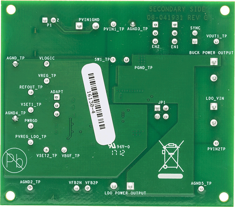
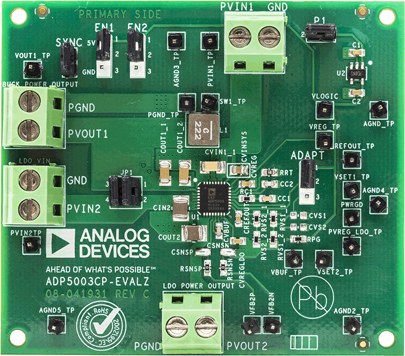
ADP5003 Evaluation Board