In-Application Programming of Sector Erasable Program, and Data Flash in a MAXQ Microcontroller
In-Application Programming of Sector Erasable Program, and Data Flash in a MAXQ Microcontroller
Abstract
This application note describes the program and data flash and how to erase/write the flash using the built-in utility ROM. This application note applies to the MAXQ flash-based microcontrollers that use a sector erasable flash.
Introduction
This application note describes how to manage the internal data and program flash for the MAXQ microcontrollers that use sector erasable flash. General information explains how to construct a boot-loader application to perform in-application programming of the program flash. Note: this document is not applicable for MAXQ microcontrollers that use a page-erasable flash, i.e., that allow small amounts of the flash to be erased. Each MAXQ data sheet describes the type of flash used on that microcontroller.
Flash Overview
Memory Maps
This application note shows flash memory map examples for various memory sizes, which do not precisely match any MAXQ part. These maps are only references for the examples in this document. Each MAXQ data sheet will list the memory map options for that part.
There is no operational difference among the boot, program, and data flash sectors. If the boot-loader application needs more space than the first flash sector provides, the application can extend into the next sector. However, labeling does differ in the examples below to illustrate how the different sectors are used in this document.
Table 1. Example of Flash Memory Maps
Data Flash
Data flash can be used to reliably store system data that needs to be programmed either once or periodically during system operation. While the size of the data flash depends on the specific MAXQ part, it is typically between 128 to 2k words.
There are limitations to using data flash. Unlike EEPROM, the data flash cannot be word erased; a complete sector must be erased at one time. Erasing a sector typically takes 0.7 seconds, but can take as long as 15 seconds under worst case conditions. During this time, user code is stalled so no other processing can occur. These limitations must be considered carefully when you select the software technique appropriate for your system requirements. For most periodic data-storage needs, a bounded queue and/or bank switching technique can meet system reliability requirements. Simple examples of the bank switching and bounded queue techniques follow below.
Bounded Queue
A bounded queue technique is a queue limited by a fixed number of items. This approach is commonly used whenever periodic data is processed. A 2k word data flash, for example, can be divided into 32 to 64 word entries, which would result in the memory map in Table 2.
Upon initialization, a startup routine can scan the queue entries to determine the next available entry in the queue. Once the queue is full, it must be erased before another entry can be written. If all entries are needed, then you must also alternate between two different sectors to maintain all the data. Once the flash is erased, the new entry can be written. The drawback to this approach is that all data can be lost if power drops during the erase process. Figure 1 illustrates the flow of entries into a bounded queue. See Appendix A for a simple C source code example.
If this bonded-queue approach does not meet system requirements, then bank switching will also be needed.
| FLASHQueue[ ] | |
| Queue Index | Data Flash Address |
| 31 | 0xF7C0-0xF7FF |
| 30 | 0xF780-0xF7BF |
| 29 | 0xF740-0xF77F |
| . . . . | . . . . |
| 2 | 0xF080-0xF0BF |
| 1 | 0xF040-0xF07F |
| 0 | 0xF000-0xF03F |

Figure 1. Bounded queue flow.
Bank Switching
Bank switching is an effective method for preventing data loss or corruption during the long sector erase cycles. For this document, the term 'Bank' is equivalent to the term 'Sector.' Bank switching works well when the sector size is slightly larger than the total data size. The negative to bank switching is that it requires minimally two sectors of data flash. When the total data size to be written is much smaller than the sector size, the best approach combines the bank switching and bounded queue methods.
If bank switching is necessary for the application, then select a version of the MAXQ with at least two data-flash sectors. Table 3 shows an example memory map of two 1K x 16 flash sectors. Figure 2 illustrates the bank switching write/erase flow.
See Appendix A for a simple C source code example.
| Flash Sectors | |
| Sector Number | Data Flash Address |
| 0 | 0xF000-0xF3FF |
| 1 | 0xE000-0xE3FF |
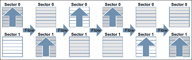
Figure 2. Bank switching flow.
Bounded Queue and Bank Switching Together
Using bounded queue and bank switching together is the most reliable and flexible approach for managing data flash. Their combination works well when small amounts of data need to be stored to flash periodically and data integrity must be maintained. Table 4 shows an example memory map of two 2K x 16 sectors divided into 32 equal entries. Figure 3 illustrates the flow of data in the bounded queue between two sectors.
The coding for this combined approach is only slightly more complex than bounded queue alone. See Appendix A for a simple C source code example.
| FQueueBank0[ ] | FQueueBank0[ ] | ||
| Queue Index | Data Flash Address | Queue Index | Data Flash Address |
| 31 | 0xF7C0-0xF7FF | 31 | 0xE7C0-0xE7FF |
| 30 | 0xF780-0xF7BF | 30 | 0xE780-0xE7BF |
| 29 | 0xF740-0xF77F | 29 | 0xE740-0xE77F |
| . . . . | . . . . | . . . . | . . . . |
| 2 | 0xF080-0xF0BF | 2 | 0xE080-0xE0BF |
| 1 | 0xF040-0xF07F | 1 | 0xE040-0xE07F |
| 0 | 0xF000-0xF03F | 0 | 0xE000-0xE03F |

Figure 3. Bounded queue and bank switch flow.
Utility ROM Flash Routines
To program, erase, and verify flash, the MAXQ microcontrollers have on-chip flash-support routines residing in ROM (read-only memory). There are two ways to access these routines. Direct access, the first and fastest method, directly calls the routine by providing a header file with the following lines:
u16 flashEraseSector(void *);
u16 flashEraseAll(void);
u16 flashWrite(u16 *pAddress, u16 iData);
Then add linker defines to assign the appropriate address for each routine. For the IAR linker file, the added lines would look like this:
-DflashEraseSector=0x8XXX
-DflashEraseAll=0x8XXX
-DflashWrite=0x8XXX
Replace 0x8XXX with the appropriate memory address for each routine. Other compilers may use a different method for adding these references.
Note that the direct access method does not provide forward compatibility with future ROM versions.
The second method uses table lookup. Although this method provides greater compatibility, it consumes more time to execute. After each routine description below, an assembly routine uses the table-lookup method to obtain the address of the ROM Utility routine. Table 5 shows the flash routines supplied by the Utility ROM. For a complete listing of ROM Utility routines, reference the User's Guide for the specific MAXQ part used.
| Routine Number | Routine Name | Entry Point ROMTable = ROM[800Dh] |
Entry Point Physical Address |
| 2 | flashEraseSector | ROM[ROMTable + 1] | 0x8XXX |
| 3 | flashEraseAll | ROM[ROMTable + 2] | 0x8XXX |
| 15 | flashWrite | ROM[ROMTable + 14] | 0x8XXX |
| Routine | u16 flashWrite(u16 *pAddress, u16 iData) |
| Summary | Programs a single word of flash memory. |
| Inputs | A[0] - Word address in flash memory to which to write. A[1] - Word value to write to flash memory. |
| Outputs | Carry: Set on error and cleared on success. If set, then A[0] contains one of the following error codes: 1 : failure due to software timeout 2 : failure reported by hardware (DQ5/FERR) 4 : command not supportedSW_FERR - Set on error, cleared on success. |
| Notes | The watchdog must not be active, or the watchdog timeout must be set long enough to complete this routine without triggering a reset. |
The following assembly code example calls the flashWrite() utility routine using the indirect addressing method (lookup table). This routine is called by C code.
; This routine is callable by C code using the following prototype
; u16 flashWrite(u16 *pAddress, u16 iData);
;
flashWrite:
    move APC, #0           ; No auto inc/dec of accumulator.
    move AP,  #2           ; Set ACC to A[2]
    move DP[0], #0800Dh    ; This is where the address of the table is stored.
    move ACC, @DP[0]       ; Get the location of the routine table.
    add  #14               ; Add the index to the flashWrite routine.
    move DP[0], ACC
    move ACC, @DP[0]       ; Retrieve the address of the routine.
    call ACC               ; Execute the routine.
    ret                    ; Status returned in A[0]
| Routine | u16 flashEraseSector(void *pAddress) |
| Summary | Erases a single sector of flash memory |
| Inputs | A[0] - Address located in the sector to erase. |
| Outputs | Carry: Set on error and cleared on success. If set, then A[0] contains one of the following error codes: 1 : failure due to software timeout 2 : failure reported by hardware (DQ5/FERR) 4 : command not supported SW_FERR - Set on error, cleared on success. |
| Notes | The watchdog must not be active, or the watchdog timeout must be set long enough to complete this routine without triggering a reset. |
; This routine is callable by C code using the following prototype
; u16 flashEraseSector(void *pAddress);
;
flashEraseSector:
    move APC, #0           ; No auto inc/dec of accumulator.
    move AP,  #1           ; Set ACC to A[1]
    move DP[0], #0800Dh    ; This is where the address of the table is stored.
    move ACC, @DP[0]       ; Get the location of the routine table.
    add  #1                ; Add the index to the flashEraseSector routine.
    move DP[0], ACC
    move ACC, @DP[0]       ; Retrieve the address of the routine.
    call ACC               ; Execute the routine.
    ret                    ; Status returned in A[0]
| Routine | void flashEraseAll(void) |
| Summary | Erases the entire program and data flash memory, including the boot loader sector. This routine is not normally used for IAP, as great care must be taken to ensure that the erase/programming sequence is not interrupted. |
| Inputs | None |
| Outputs | Carry: Set on error and cleared on success.SW_FERR: Set on error, cleared on success. |
| Notes | The watchdog must not be active, or the watchdog timeout must be set long enough to complete this routine without triggering a reset. |
; This routine is callable by C code using the following prototype
; void flashEraseAll(void);
;
flashEraseAll:
    move APC, #0           ; No auto inc/dec of accumulator.
    move AP,  #0           ; Set ACC to A[0]
    move DP[0], #0800Dh    ; This is where the address of the table is stored.
    move ACC, @DP[0]       ; Get the location of the routine table.
    add  #2                ; Add the index to the flashEraseAll routine.
    move DP[0], ACC
    move ACC, @DP[0]       ; Retrieve the address of the routine.
    call ACC               ; Execute the routine.
    ret
In-Application Programming
An important requirement for most flash-based systems is the ability to update firmware while the system is installed in the end product. This is referred to as In-Application Programming (IAP). This section will outline general guidelines for creating an IAP application.
The Utility ROM flash routines outlined above perform all the actions necessary to erase and write the flash ROM. It is thus possible for an end-user application to perform operations on the flash memory. Like any other subroutine call, control will return to the end-user's code after completion of the routine.
For a reliable IAP, the boot-loader application must be separate from the main application. This ensures that the reprogramming procedure can be retried after an incomplete reprogramming sequence.
Boot Loader
Because the ROM jumps to address 0x0000 after initialization, the entry point of the boot-loader application must be placed at 0x0000. The boot-flash sector size varies depending on the MAXQ part selected. The boot-loader application can extend into as many flash sectors as needed, and any sector used will not be available for the user's application code. The specific requirements that must be met when erasing and writing flash are listed in Table 6.
| You cannot erase or program from the same flash sector from which you are executing code. This is not normally a problem since the flash Boot Sector should never be erased during IAP. |
| The watchdog must not be enabled or the watchdog timeout must be set long enough to complete this routine without triggering a reset before the flashEraseSector() routine is called. If the watchdog time out occurs before the erase is complete, it will reset the part. Erasing a sector typically takes 0.7 seconds; it can take up to 15 seconds under worst case conditions. |
| Since the System Control Register bit SC.UPA must be set to 0 to access the Utility ROM, a ROM Utility routine cannot be called directly from program memory addresses = 0x8000. If access to a Utility ROM routine is required from a program in upper memory (= 0x8000), the program must indirectly call the ROM routine through a routine residing in lower memory (<0x8000). This effectively limits the boot loader to = 64kB (32kB x 16). |
The flowchart in Figure 4 shows what the MAXQ does when exiting the reset state. After a diagnostic of the ROM itself and verification that the flash is ready, the ROM initialization code jumps directly to address 0x0000. Read the appropriate data sheet and User's Guide to verify that your MAXQ microcontroller follows this boot sequence.

Figure 4. Simplified ROM initialization flowchart.
The flowchart in Figure 5 shows what a simple boot-loader application can look like. When using a boot loader for IAP, the entry point for the main application will typically be at address 0x2000 + Header Offset for the 16kB (8K x 16) boot-loader option, and at address 0x4000 + Header Offset for the 32kB (16K x 16) boot-loader option. A simple application header will be similar to the following:
typedef struct {
    u16 iSize;  // The size of the application in words
    u32 iCRC;   // The CRC of the application
    u8 ID[8];   // ID string for current application
} APPLICATION_HEADER;
Using the information from this header, the boot loader can check the validity of the main application program and report the version identification, if requested.

Figure 5. Simplified flash boot-loader flowchart.
The programming sequence itself is quite simple. Erase each sector containing the main application code through a call to flashEraseSector(). Then write one word at a time by calling flashWrite() for every word to be programmed. You should erase the block containing the application header first, and program the CRC data last to minimize the possibility of an errant CRC match. A simple routine to reflash the microcontroller that gets data through the serial port can look like the following:
/*
// VerySimpleReFlash()
//    As simple as it gets.
//    Step 1. Wait for erase command, then erase flash.
//    Step 2. Wait for program command, then program flash one word
//            at a time.
*/
void VerySimpleReFlash()
{
u16 iStatus;             // The status returned from flash utility ROM calls
u16 iSize;               // The size of the main code to program
u16 *pAddress = 0x2000;  // The starting address of the main application

    InitializeCOMM();    // Can be CAN or UART
    WaitForEraseCommand();

    SlowDownWatchdog();  // If watchdog enabled set update > 15s

    iStatus = flashEraseSector(C_ADDRESS_SECTOR_1);
    if (iStatus == 0)
        iStatus = flashEraseSector(C_ADDRESS_SECTOR_2);

    UpdateWatchdog();    // Prevent watchdog timeout

    SendFlashErasedResponse(iStatus);

    if (iStatus)
        ResetMicro();

    iSize = WaitForProgramCommand();
    while (iSize--)
    {
        u16 iData = GetWordFromCOMM();
        iStatus = flashWrite(pAddress, iData);
        if (iStatus)
            break;
        ++pAddress;
        UpdateWatchdog();    // Prevent watchdog timeout
    }

    SendFlashWriteResponse(iStatus);
    ResetMicro();
}
Remember that any program space not used by the boot-loader application can be used for other routines and/or constant data storage. A good example of this would be storing all the routines for indirectly calling Utility ROM routines, such as the ones listed in the Utility ROM Flash Routines section above. There is one restriction to storing other information in the same sector as the boot loader: it cannot be erased without erasing all or part of the boot-loader application itself.
IAP Using a RAM-Based Flash Routine
A RAM-based flash routine can be used to reflash the MAXQ microcontroller when fault recovery is not required. This method requires that the main application copy a small relocatable flash programming routine into RAM and then jump to the routine. Table 7 shows several restrictions to consider when executing code from RAM.
| SC.UPA must be set to 0 before executing a RAM-based routine. This means that the application must jump to the RAM routine from the code segments P0 & P1. |
| RAM cannot be accessed as data and program at the same time. This means that only the registers and hardware stack are available for data storage. |
| The Interrupt Vector must point to a RAM routine if interrupts are enabled. Typically interrupts are turned off and polling is used due to the simplicity of the RAM reflash routine. |
Typically the flash routine will communicate through either the UART or CAN interface. To allow a more robust error-recovery mechanism, it is usually best to receive small packets of data and send some kind of acknowledgement. Figure 6 charts how a reflash routine can flow. Remember, if reprogramming is not successfully completed before loss of power, the microcontroller will need to be reprogrammed through the JTAG port.

Figure 6. Simplified RAM reflash routine flowchart.
Appendix A. Code Examples
Download: Appendix A (PDF)