Wide Input Range, High Efficiency Step-Down Switching Regulators
Introduction
The LT1676 and LT1776 are Linear Technology’s latest offerings for high efficiency step-down switching regulator applications. These two parts are pin-for-pin compatible and virtually identical in operation, the only difference being their internal oscillator frequencies—100kHz for the LT1676 vs 200kHz for the LT1776. They operate in a fixed frequency mode (as opposed to constant off-time or on-time, for instance) and can be externally synchronized to a higher switching frequency.
The internal output switch is rated at a nominal peak current of 700mA, which typically accommodates DC output currents of up to 500mA. The input voltage range is 7.4V to 60V. Maintaining acceptable efficiency in the upper half of this input voltage range requires very fast output-switch edge rates. The LT1676/LT1776 contain specialized output circuitry to deliver this performance. Additionally, they contain circuitry to monitor output load level and reduce leading-edge switch rate (turn-on) when the output load is light. This arrangement helps avoid pulse skipping at light load, with its consequent subharmonic behavior.
True current mode operation is supported, with all its well known advantages for switching regulator operation. The shutdown pin implements a pair of functions. Pulling it down to near ground turns off the part almost completely and reduces the quiescent current to a few tens of microamperes. The second shutdown pin function acts at a threshold of roughly 1.25V. Below this level, the part operates normally, except that output switching action is inhibited. This allows the implementation of an undervoltage lockout function set by, for instance, an external resistor divider. The LT1676/LT1776 are available in both 8-pin SO and PDIP packages.
Theory of Operation
The LT1676/LT1776 are current mode switching regulator ICs optimized for high efficiency operation in high input voltage, low output voltage buck topologies. The block diagram in Figure 1 shows an overall view of the system. Several of the blocks are straightforward and similar to those found in traditional designs, including the internal bias regulator, oscillator and feedback amplifier. The novel portion includes an elaborate output switch section and a logic section to provide the control signals required by the switch section.

Figure 1. LT1776 block diagram.
The LT1676/LT1776 operate much the same as traditional current mode switchers, the major difference being their specialized output switch section. Due to space constraints, this discussion will not reiterate the basics of current mode switcher/controllers and the step-down topology. A good source of information on these topics is Linear Technology Application Note 19.
One of the classic problems in delivering low output voltage from a high input voltage at good efficiency is that minimizing AC switching losses requires very fast voltage (dV/dt) and current (dI/dt) transitions at the output device. This is in spite of the fact that in a cost-effective bipolar IC process implementation, slow lateral PNPs must be included in the switching signal path.
Fast, positive-going slew rate action is provided by lateral PNP Q3 driving the Darlington arrangement of Q1 and Q2. The extra β available from Q2 greatly reduces the drive requirements of Q3. Although desirable for dynamic reasons, this topology alone will yield a large DC forward voltage drop. A second lateral PNP, Q4, acts directly on the base of Q1 to reduce the voltage drop after the slewing phase has taken place. To achieve the desired high slew rate, PNPs Q3 and Q4 are “force-fed” packets of charge via the current sources controlled by the BOOST signal.
Please refer to the timing diagram of Figure 2a. A typical oscillator cycle is as follows: The logic section first generates a SWDR signal, which powers up the current comparator and allows it time to settle. About 1µs later, the SWON signal is asserted and the BOOST signal is pulsed for a few hundred nanoseconds. After a short delay, the VSW pin slews rapidly to VIN. Later, after the peak switch current, indicated by the control voltage VC, has been reached (current mode control), the SWON and SWDR signals are turned off and SWOFF is pulsed for a few hundred nanoseconds. The use of an explicit turn-off device (Q5) improves turn-off response time and thus aids both controllability and efficiency.

Figure 2a. Timing diagram: high dV/dt mode.
The system described previously handles heavy loads (continuous mode) at good efficiency, but is actually counterproductive for light loads. The method of jamming charge into the PNP bases makes it difficult to turn them off rapidly and achieve the very short switch ON times required by light loads in discontinuous mode. Furthermore, the high leading edge dV/dt rate has a similar adverse effect on light load controllability.
The solution is to employ a “boost comparator” whose inputs are the VC control voltage and a fixed internal threshold reference, VTH. (Remember that in a current mode switching topology, the VC voltage determines the peak switch current.) When the VC signal is above VTH, the previously described “high dV/dt” action is performed. When the VC signal is below VTH, the BOOST pulses are absent, as can be seen in Figure 2b. Now the DC current activated by the SWON signal alone drives Q4 and this transistor drives Q1 by itself. The absence of a BOOST pulse plus the lack of a second NPN driver results in a much lower slew rate, which aids light load controllability.

Figure 2b. Timing diagram: low dV/dt mode.
A further aid to overall efficiency is provided by the specialized bias regulator circuit, which has a pair of inputs, VIN and VCC. The VCC pin is normally connected to the switching supply output. During start-up conditions, the LT1676/LT1776 power themselves directly from VIN. However, after the switching supply output voltage reaches about 2.9V, the bias regulator uses this supply as its input. Previous generation step-down controller ICs without this provision typically required hundreds of milliwatts of quiescent power when operating at high input voltages. This both degraded efficiency and limited available output current due to internal heating.
Choosing Between the LT1676 and LT1776
As previously mentioned, the LT1676 and LT1776 devices are pin-for-pin compatible and, in fact, nearly identical. The only real difference is in their internal oscillator frequencies, nominally 100kHz for the LT1676 and 200kHz for the LT1776. A user must decide which version is best suited for his or her particular application. Generally, the LT1776 is favored, as its higher switching frequency allows for a lower valued and possibly physically smaller and less costly inductor. However, the higher switching frequency of the LT1776 increases AC switching losses, adversely affecting efficiency and internal power dissipation. In fact, certain combinations of high input voltage and output current may yield unacceptable internal power dissipation and consequent thermal rise. In these cases, the slower switching frequency of the LT1676 may yield acceptable operation. (A more thorough treatment of input voltage vs operating frequency considerations can be found in the LT1776 data sheet.)
Applications
Minimum Component-Count Application
Figure 3a shows a basic “minimum component count” application using the LT1676. The circuit produces 5.0V at up to 500mA IOUT with input voltages in the range of 12V to 48V. The typical POUT/PIN efficiency is shown in Figure 3b. No pulse skipping is observed down to zero external load. (The several milliamperes drawn by the VCC pin acts as a sufficient preload.) As shown, the SHDN and SYNC pins are unused, however either (or both) can be optionally driven by external signals as desired.

Figure 3a. Minimum component-count application.

Figure 3b. Efficiency of Figure 3a’s circuit.
Minimum PC Board Area Application
The previous application example used the LT1676 to demonstrate simultaneously the maximum input voltage and output current capability. As such, the input bypass capacitor choice was a high frequency aluminum electrolytic type, rated to 63V. Also, the 100kHz switching rate of the LT1676 requires an inductor of about 220µH. The DO3316 device size was chosen to support the output current requirements. However, both of these components are physically large.
The application example in Figure 4a shows a circuit that is much smaller physically than the previous minimum component count application. The nominal 200kHz switching frequency of the LT1776 allows the use of a physically smaller 68µH inductor—a Coilcraft DO1608C-683. This inductor will support output current to 400mA at 5V. However, the part is incapable of withstanding an indefinite short circuit to ground. (Momentary shorts of a few seconds or less can still be tolerated.) Additionally, the bulky aluminum electrolytic capacitor previously on VIN has been replaced by a compact 35V-rated tantalum type. The result is a postage-stamp-sized circuit with efficiency as shown in Figure 4b.

Figure 4a. Minimum PC board area application.

Figure 4b. Efficiency of Figure 4a’s circuit.
Burst Mode Application
The minimum component count application demonstrates that power supply efficiency degrades with lower output load current. This is not surprising, as the LT1676 itself represents a fixed power overhead. A possible way to improve light load efficiency is to use Burst Mode™ operation.
Figure 5a shows the LT1676 configured for Burst Mode operation. Output voltage regulation is now provided in a “bang-bang” digital manner, via comparator U2, an LTC1440. Resistor divider R4/R5 provides a scaled version of the output voltage, which is compared against U2’s internal reference. Intentional hysteresis is set by the R6/R7 divider. As the output voltage falls below the regulation range, the LT1676 is turned on. The output voltage rises and, as it climbs above the regulation range, the LT1676 is turned off. Efficiency is maximized as the LT1676 is only powered up while it is providing heavy output current. Figure 5b shows that efficiency is typically maintained at 75% or better down to a load current of 10mA. Even at a load current of 2mA, efficiency is still a respectable 65% to 75% (depending on VIN).

Figure 5a. Burst Mode operation configuration.

Figure 5b. Efficiency of Figure 5a’s circuit.
Resistor divider R1/R2 is still present, but does not directly influence output voltage. It is chosen to ensure that the LT1676 delivers high output current throughout the voltage regulation range. Its presence is also required to maintain proper short-circuit protection. Transistors Q1 and Q2 and resistor R7 form a high VIN, low quiescent current voltage regulator to power U2.
Battery Charger Application
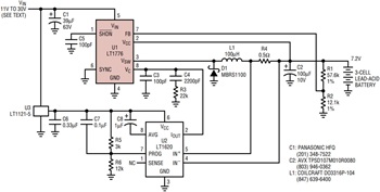
Figure 6a shows the LT1776 configured as a constant-current/constant-voltage battery charger. An LT1620 rail-to-rail current sense amplifier (U2) monitors the differential voltage across current sense resistor R4. As this equals and exceeds the voltage across resistor R5 in the R5/R6 divider, the LT1620 responds by sinking current at its IOUT pin. This is connected to the VC control node of the LT1776 and therefore acts to reduce the amount of power delivered to the load. The overall constant-current/constant-voltage behavior can be seen in Figure 6b.

Figure 6a. Wide VIN range, high efficiency battery charger.

Figure 6b. Battery charger output voltage vs output current for Figure 6a’s circuit.
Target voltage and current limits are independently programmable. The output voltage of 7.2V, which corresponds to the charging voltage of a 3-cell lead-acid battery, is set by the R1/R2 divider and the internal reference of the LT1776. Output current, presently 200mA, is set by current sense resistor R4 and the R5/R6 divider. (A 16-pin version of the LT1620 that implements end-of-cycle detection is also available. This is useful for implementing lead-acid battery “top-off” charger behavior or the like. See the LT1620 data sheet for further information.)
The circuit as shown accommodates an input voltage range of 11V to 30V. The upper input voltage limit of 30V is determined not by the LT1776, but by the LT1121-5 regulator (U3). (A regulated 5V is required by the LT1620.) This regulator was chosen for its micropower behavior, which helps maintain good overall efficiency. However, the basic catalog part is only rated to 30V. Substitution of the industry standard LM317, for example, extends the allowable input voltage to 40V (or more with the HV version), but its greater quiescent current drain degrades efficiency from that shown.
Dual Output SEPIC Converter
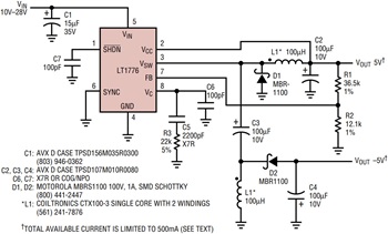
All of the previous applications provide a single positive output voltage. Real world situations often require dual supply voltages. The SEPIC topology (single-ended primary inductance converter) offers a cost-effective way to simultaneously generate a negative voltage with a single piece of magnetics. The circuit in Figure 7 uses an LT1776 to generate both positive and negative 5V. The two inductors shown are actually just two windings on a standard Coiltronics inductor. Capacitor C3 creates the SEPIC topology, which improves regulation and reduces ripple current in L1.

Figure 7. Dual-output SEPIC converter.
For the best negative supply voltage regulation, this output should have a preload of at least 1% of the maximum positive load. Total available current from both outputs is limited to 500mA. Maximum negative supply current is limited by the positive 5V load. A typical limit is one-half of the positive current, but a more exact calculation includes the input voltage. For this and further details of this topology, see Linear Technology Design Note 100.
Positive-to-Negative Converter
The previous example used a dual inductor to create a pair of output voltages, one positive and the other negative. The positive-to-negative converter topology illustrated in Figure 8 generates a single negative output voltage from a positive input voltage, using just an ordinary inductor. The topology is somewhat similar to the original step-down arrangement, but the inductor is grounded and the LT1776 ground is now referred to the negative output voltage. Note that the integrated circuit must now be rated for the worst case sum of the input voltage plus the absolute value of the output voltage. The relatively high input voltage rating of the LT1676/LT1776 parts along with their good efficiency under such conditions make them an excellent choice for implementing this topology. The circuit as shown converts an input voltage in the range of 10V to 28V to a –5V output. Available output current is 300mA at the worst case VIN of 10V.

Figure 8. Positive-to-negative converter.
The user should exercise caution in modifying this circuit for other applications. The positive-to-negative topology is not as straightforward as the step-down topology. It is actually more like a flyback topology, in that current is delivered to the output in discrete pulses. The output capacitor must supply the entire load current for at least a portion of the switching cycle, so output capacitor ripple current rating and ESR may be an issue. Maximum available output current will usually be a strong function of input voltage. Supporting low VIN-to-VOUT ratios may require additional components for maintaining control-loop stability. A detailed theoretical analysis of this topology and its behavior can be found in Linear Technology Application Note 44.
Conclusion
The LT1676 and LT1776 provide excellent efficiency in high input voltage/low output voltage switching regulator applications. This LT1776’s 8-pin SO package and 200kHz switching rate are especially useful in implementing compact power supply solutions. These devices’ innate ability to avoid pulse skipping under light loads, plus the optional sync function, aid in controlling the frequency spectrum of switching-generated noise.


