Near Noiseless ADC Drivers for Imaging
CCDs (charge coupled devices) and other sensors place heavy demands on digitizers, both in terms of sample rates, and in signal-to-noise ratio. The sensor output is typically a ground-referenced series of analog levels (pixels), possibly with transients occurring between the pixel boundaries. As the number of pixels increases, so does the sample rate of the ADC required to capture the image, with 20Msps pipelined ADCs sufficient for most high dynamic range applications. To ensure the highest SNR performance of the sampled signal, the drive circuitry for the ADC must provide low impedance, fast settling without introducing wideband noise and yet present high input impedance to the sensor.
This article presents an interface circuit between the sensor and a high performance ADC that does not compromise the SNR performance. The LTC2270 16-bit pipelined ADC family is intended for high end imaging applications. The 84.1dB SNR of this family makes it attractive for imaging, but it also features very good SFDR—over 100dB. The input range is 2.1VP-P, significantly less than the output of most imaging devices, so attenuation and level-shifting is required.
The inputs of these ADCs must be driven with a well-balanced differential drive. The single ended drive normally available from the sensor would force the internal virtual grounds to absorb common mode input current, which would cause degraded performance. These ADCs are also very low powered devices at 80mW/channel. Differential drive is actually fundamental to the low power operation since single ended drive would require additional power to maintain a stable internal reference point in the ADC. These devices operate on 1.8V supplies, imposing an input range of this order, if nothing else, simply to stay away from the rails. It is important to stay away from the rails to prevent differential phase error that would be associated with the voltage variable capacitance of internal protection diodes.
Therein lies a dilemma: A differential amplifier capable of performing single ended to differential translation without compromising the SNR of the ADC will necessarily have low input impedance (or low value resistors) and as it must settle quickly to 16-bit accuracy, will likely consume something on the order of four times the power of the ADC itself. The LTC6409 differential amplifier is an example that produces good results, but consumes 260mW, requiring that the surrounding network dissipate about 40mW just to produce a level shift. Furthermore, it dissipates signal power in the relatively low value resistors required for low noise and for maintaining phase margin.
These differential amplifiers as a result have low input impedance. The buffer that would be required to present a high impedance to the CCD also presents a dilemma. It must be low noise, be capable of settling in less than 25nsec, and be capable of slewing with enough dV/dt to maintain closed loop operation during transients. Additionally, it must be capable of driving the low input impedance of the differential amplifier. Yet, the application demands low power. This dilemma is even greater if there is the expectation that the amplifier operate from the single supply rail.
Most differential amplifiers present a number of problems as they either need band-limiting after the amplifier to the extent that settling is compromised, or they are not very stable with a gain of less than one (a noise gain of less than two) and as such tend to ring. Many are not common mode compatible with the 1.8V ADCs or they do not have enough headroom to accommodate a double terminated filter, or a level shift after the amplifier. The LTC6404 is a good case to study. It is stable at unity gain, does not ring as do some, and could potentially be used with an attenuator after the amplifier, but the input referred noise is 1.5nV. This compares to 1.1nV for the LTC6409. The LTC6404 noise density peaks considerably above 100MHz, it consumes 175mW, and it is not really compatible with the 900mV common mode required by the LTC2270. If it were followed by a filter and level shift, the impedance would be such that you will dissipate some 80mW dropping voltage in the dividers. You could potentially operate the amplifier off +3.3V and –2V to resolve common mode compatibility and produce a larger signal swing without requiring a level shift after the amplifier. But the negative supply is not often palatable to designers.
The settling time available to the amplifier may not be an entire clock cycle. The source may dictate this, but there is a disturbance produced by the ADC on the opposite edge of the clock and this would give the filter only ½-clock cycle to settle even if the amplifier were not otherwise disturbed. If the amplifier is disturbed by this event, it does not leave as much time for the filter to settle.
A simple RC would require about 14 time constants to settle to 16 bits, and for 20Msps, this would result in a bandwidth of about 90MHz. As it happens, the amplifier will be disturbed to some extent by sampling and this means that the bandwidth of a simple post filter must be extended to 130MHz to 150MHz to allow for some settling of the amplifier in response to the disturbance. Unfortunately, this will pass noise in the region where the amplifier is peaking. A higher order filter may result in a more pronounced reduction of noise contribution from the earlier Nyquist zones, but will not necessarily settle very quickly.
The scheme described herein can drive the 25Msps LTC2270 family with 84.1dB SNR and 17pF sample capacitors. Impedances can be raised and power consumption can be reduced at sample rates of 20Msps, and less. For sample rates higher than 30Msps, a more conventional topology involving a fast buffer, followed by a differential amplifier like the LTC6409 is required. The LTC6404-1 can alternatively be used in that case.
The Near Noiseless Suggestion
The circuit in Figure 1 shows a suggested drive scheme that results in almost no loss of SNR with the LTC2270 family, yet can settle to 16 bits within 1 pixel at 25Msps. The noise at –84.0dB (all included) is such that it will not necessarily be within 1 count in a single frame, but averaging multiple frames could resolve to 16 bits.
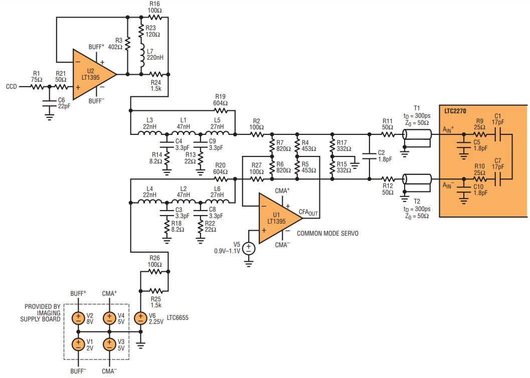
Figure 1. Near noiseless circuit for interfacing a CCD to a high performance ADC.
The buffer amplifier (U2) is a current feedback amplifier used essentially as an emitter follower. The bulk of the output current is taken via R16, seemingly from the emitters, although power is delivered from the output.
As the impedance looking into the inverting input is low compared to the feedback network, the output noise is attenuated at the inverting input and, as a result, the inverting input noise current does not contribute significantly. This amplifier has a voltage noise specification of 4.5nV/√Hz, although when used as a unity gain buffer, inverting input noise current in the minimum value feedback resistor produces 10.1nV/√Hz. However in this emitter-follower-like mode of operation, it appears to be on the order of 1.5nV/√Hz to 2nV/√Hz.
There is a feedback loop around the amplifier and this amplifier imposes a minimum feedback resistor of 400Ω. However, at low frequency, the feedback impedance is 400Ω in parallel with R23 to reduce the excursion required at the output. But at high frequency, the feedback is the required minimum 400Ω.
There is a minor amount of output power taken from the output, via R24,just to reduce the required excursion produced at the output. But this may not be required in many cases, for example where the video signal is 0V–4V, or less.
There is provision for R24 just in case, in the future, U2 may be a different amplifier where it is practical to take power from the output. There are several possible alternatives depending on required slewing. A low noise fast settling FET amplifier could possibly be used on a single supply. With rail-to-rail amplifiers, it is likely that the positive rail must be 6V to avoid crossing through the transition region between two input stages, a region that causes distortion. If the LT1395 is used, 7.5V to 8V must be used for VCC and –2V for VSS, if intended to receive 0V–5V signals.
A lower powered amplifier such as the LT6252 may be used if there is no need to settle through a full-scale step between pixels. Bad pixels however would bleed into following pixels. The presence of clock feed-through and the actual settling time available may limit these choices.
The second amplifier is also an LT1395, but note that this cannot be a dual LTC1396, unless the application were to involve signals centered on ground potential. This second stage must operate on 5V and –5V in order to sink current and perform a level shift from ~2.5V common mode to 0.9V common mode, as well as provide differential drive by virtue of controlling the common mode. The noise and distortion contribution of this amplifier is largely rejected by the CMRR of the ADC as its influence is only common mode, assuming the network surrounding the amplifier is completely symmetrical.
We developed a power supply board that provides all four of the required voltages from a single 5V input. The power supply circuit is capable of powering four channels, yet produces no evidence of the 1.2MHz switching rate used by the LT3471—even at –125dBFS.
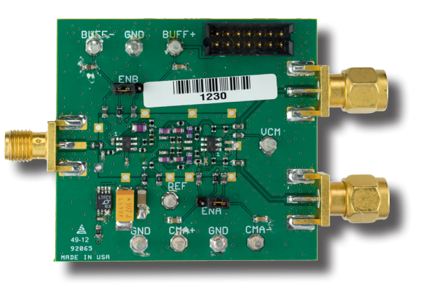
Figure 2. Prototype imaging board.
As shown, this driver produces 84.0dB SNR combined with the ADC and including any contribution from the power supply board. The tests below were done with R1 at 75Ω, and a 50Ω source. This circuit should be suitable where CCDs either have an output impedance in the 50Ω–200Ω range, or where the charge transfer into a holding cap produces an effective impedance in the hundreds of ohms. The use of a fast FET buffer may allow very high source impedance.
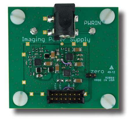
Figure 3. Prototype 0.5 square inch 4-output power supply.
The capacitor C6, at 22pF, is required if the dV/dt during transients from the CCD exceeds the slew rate of the LTC1395 or if RFI is present. CCDs appear to tolerate capacitive loads of this magnitude. If the output stage of the LTC1395 is not capable of keeping up, conduction of input protection diodes would greatly reduce the input impedance. This conduction occurs in almost any feedback amplifier. And this would produce an error if a charge transfer mechanism were exposed to this input current, possibly even if buffered in the CCD. R21 is potentially desirable as source termination if the distance between C6 and the amplifier were extended.
This topology is only practical with ADCs that have approximately 2VP-P input range and where the CCD signal is on the order of 0V–4V or 0V–5V. This takes advantage of the attenuation that is required to produce the balun action by controlling the common mode. This is analogous to the transmission line balun where high common mode impedance between input and output ports results in balanced drive if symmetrically terminated to AC ground.
The filter as shown produces a Gaussian like response, and is 3dB down at about 40MHz. The filter is replicated twice independently, in order to provide a symmetrical network that maintains the error contribution of U1 as common mode.
R7, R4, and R17 and their counterparts satisfy the requirements for stability of U1, produce attenuation of the 0V–5V signal to ±1V, and produce a level shift. These elements can in fact be after the ADC and act as end termination, which allows somewhat faster settling. If there is a significant distance between the CCD and the ADC, simulation says that the transmission path can be extended between a pair of 50Ω resistors replacing R16. If the distance is between 30cm and up to about 60cm, the cable should be 75Ω. The source termination resistor would then be 75Ω and the other side, 25Ω. PCB traces should be higher than 75Ω if possible.
If this is intended to drive into the LTC2185, for example, a 350psec transmission path is possible. If the LTC2270 family is used, the 17pF sample capacitors require that this transmission line (T1 and T2 in Figure 1) should be less than 40psec (about 1cm).
Tests performed to satisfy that this will perform with CCD signals, besides digitizing small offset frequencies from ¼FS and ½FS at 20Msps and 25Msps, include: 300kHz –1dBFS sinusoid (–92dB SFDR 2nd and 3rd), representative of dV/dt in a CCD signal; as well as a near full scale square wave (10MHz and 5MHz) with a superimposed –20dB sinusoid at 200kHz, showing no distortion on the sinusoid resulting from the large synchronous excursion in pairs of “black and white pixels.”
Note the appearance of two waveforms in the time domain plot in Figure 4, caused by alternation between the two levels in the square wave every other sample.
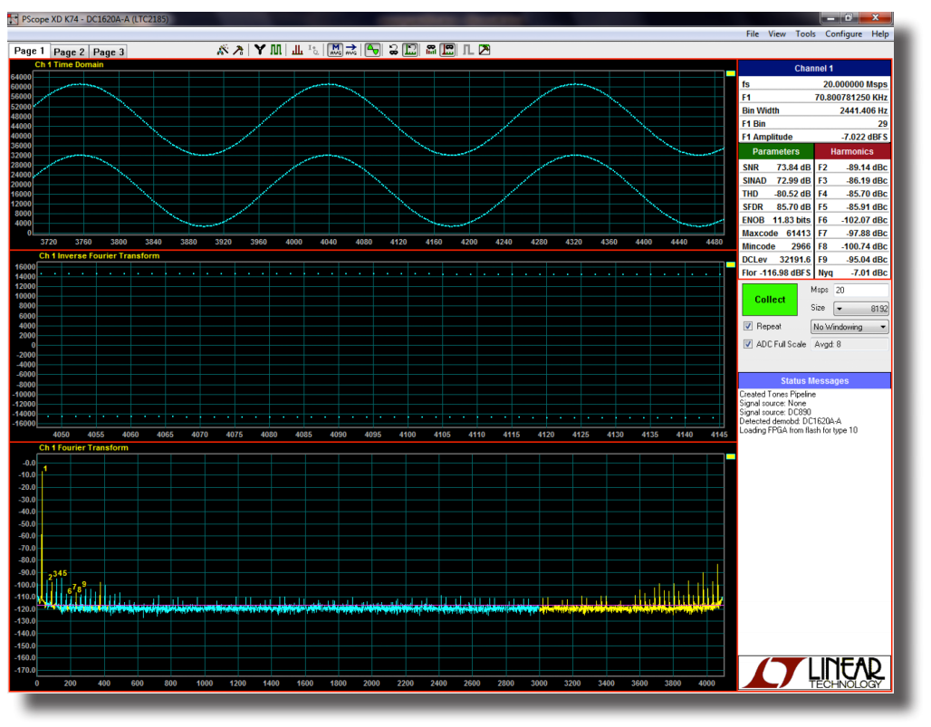
Figure 4. Two tone test –7.022dBfs sinusoid at 70kHz, –7.01dB synchronous square wave at Nyquist.
The inverse FFT window is zoomed in on the time axis, showing only the tone at Nyquist, this by selectively masking out the power in the 70kHz area.
Figure 5 shows no apparent power change in the low frequency tone, still at –7.022dBFS and only relatively minor change in the distortion components. This proves the addition of a high amplitude square wave is not causing compression at the peaks. A 70kHz tone, superimposed on a ½FS square wave is believed to represent the dV/dt and settling scenario that would be representative of that seen in a CCD waveform sampled near the end of the pixel.
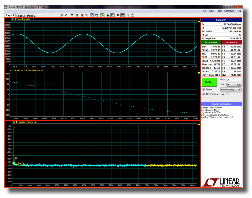
Figure 5. Same applied power level at 70kHz, but removal of power at Nyquist.
Conclusion
If an ADC with high SNR is required in an imaging application, a single-ended to differential conversion is required to get the signal from the CCD to the ADC. The conversion must attenuate the signal swing and provide a very stable common mode output level without adding significant noise. The circuit presented here can do just that. Working with a low power ADC that has a data sheet SNR specification of 84.1dB, this circuit achieved 84.0dB—implying that the conversion was nearly noiseless.


