How to Use the LTC6900 Low Power SOT-23 Oscillator as a VCO
Introduction
The LTC6900 is a precision low power oscillator that is extremely easy to use and occupies very little PC board space. It is a lower power version of the LTC1799, which was featured in the February 2001 issue of this magazine.
The output frequency, fOSC, of the LTC6900 can range from 1kHz to 20MHz—programmed via an external resistor, RSET, and a 3-state frequency divider pin, as shown in Figure 1.

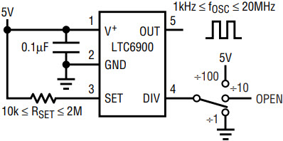
Figure 1. Basic connection diagram.
A proprietary feedback loop linearizes the relationship between RSET and the output frequency so the frequency accuracy is already included in the expression above. Unlike other discrete RC oscillators, the LTC6900 does not need correction tables to adjust the formula for determining the output frequency.
Figure 2 shows a simplified block diagram of the LTC6900. The LTC6900 master oscillator is controlled by the ratio of the voltage between V+ and the SET pin and the current, IRES, entering the SET pin. As long as IRES is precisely the current through resistor RSET, the ratio of (V+ – VSET) / IRES equals RSET and the frequency of the LTC6900 depends solely on the value of RSET. This technique ensures accuracy, typically ±0.5% at ambient temperature.
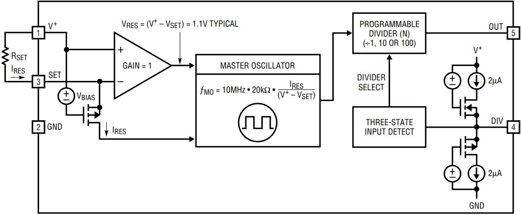
Figure 2. Simplified block diagram.
As shown in Figure 2, the voltage of the SET pin is controlled by an internal bias, and by the gate to source voltage of a PMOS transistor. The voltage of the SET pin (VSET) is typically 1.1V below V+.
Programming the Output Frequency
The output frequency of the LTC6900 can be programmed by altering the value of RSET as shown in Figure 1 and the accuracy of the oscillator will not be affected. The frequency can also be programmed by steering current in or out of the SET pin, as conceptually shown in Figure 3. This technique can degrade accuracy as the ratio of (V+ – VSET) / IRES is no longer uniquely dependent on the value of RSET, as shown in Figure 2. This loss of accuracy will become noticeable when the magnitude of IPROG is comparable to IRES. The frequency variation of the LTC6900 is still monotonic.

Figure 3. Concept for programming via current steering.
Figure 4 shows how to implement the concept shown in Figure 3 by connecting a second resistor, RIN, between the SET pin and a ground referenced voltage source VIN.
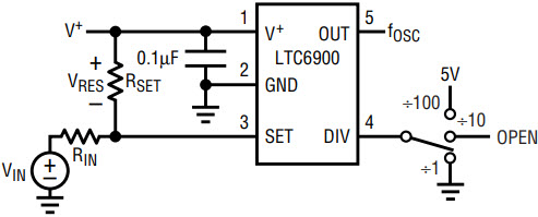
Figure 4. Implementation of the concept shown in Figure 3.
For a given power supply voltage in Figure 4, the output frequency of the LTC6900 is a function of VIN, RIN, RSET, and (V+ – VSET) = VRES:
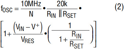
When VIN = V+ the output frequency of the LTC6900 assumes the highest value and it is set by the parallel combination of RIN and RSET. Also note, the output frequency, fOSC, is independent of the value of VRES = (V+ – VSET) so, the accuracy of fOSC is within the datasheet limits.
When VIN is less than V+, and especially when VIN approaches the ground potential, the oscillator frequency, fOSC, assumes its lowest value and its accuracy is affected by the change of VRES = (V+ – VSET). At 25°C VRES varies by ±8%, assuming the variation of V+ is ±5%. The temperature coefficient of VRES is 0.02%/°C.
By manipulating the algebraic relation for fOSC above, a simple algorithm can be derived to set the values of external resistors RSET and RIN, as shown in Figure 4:
- Choose the desired value of the maximum oscillator frequency, fOSC(MAX), occurring at maximum input voltage VIN(MAX) ≤ V+.
- Set the desired value of the minimum oscillator frequency, fOSC(MIN), occurring at minimum input voltage VIN(MIN) ≥ 0.
- Choose VRES = 1.1 and calculate the ratio of RIN/RSET from the following:
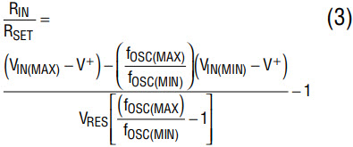
Once RIN/RSET is known, calculate RSET from:
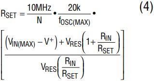
Example 1: In this example, the oscillator output frequency has small excursions. This is useful where the frequency of a system should be tuned around some nominal value.
Let V+ = 3V, fOSC(MAX) = 2MHz for VIN(MAX) = 3V and fOSC(MIN) = 1.5MHz for VIN=0V. Solve for RIN/RSET by equation (3), yielding RIN/RSET = 9.9/1. RSET = 110.1kΩ by equation (4). RIN = 9.9RSET = 1.089MΩ. For standard resistor values, use RSET = 110kΩ (1%) and RIN = 1.1MΩ (1%). Figure 5 shows the measured fOSC vs VIN. The 1.5MHz to 2MHz frequency excursion is quite limited, so the curve fOSC vs VIN is linear.
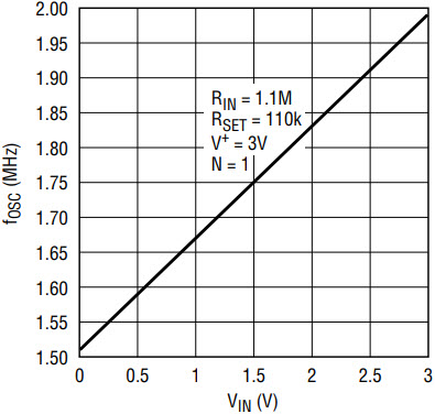
Figure 5. Output frequency vs input voltage.
Example 2: Vary the oscillator frequency by one octave per volt. Assume fOSC(MIN) = 1MHz and fOSC(MAX) = 2MHz, when the input voltage varies by 1V. The minimum input voltage is half supply, that is VIN(MIN) = 1.5V, VIN(MAX) = 2.5V and V+ = 3V.
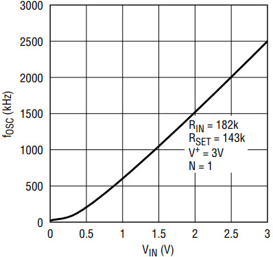
Equation (3) yields RIN/RSET = 1.273 and equation (4) yields RSET = 142.8kΩ. RIN = 1.273RSET = 181.8kΩ. For standard resistor values, use RSET = 143kΩ (1%) and RIN = 182kΩ (1%).
Figure 6 shows the measured fOSC vs VIN. For VIN higher than 1.5V the VCO is quite linear; nonlinearities occur when VIN becomes smaller than 1V, although the VCO remains monotonic.
The VCO modulation bandwidth is 25kHz that is, the LTC6900 will respond to changes in the frequency programming voltage, VIN, ranging from DC to 25kHz.
| RIN || RSET (VIN = V+) | VRES, V+ = 3V | VRES, V+ = 5V |
| 20k | 0.98V | 1.03V |
| 40k | 1.03V | 1.08V |
| 80k | 1.07V | 1.12V |
| 160k | 1.1V | 1.15V |
| 320k | 1.12V | 1.17V |
| VRES = Voltage across RSET | ||
Note:
All of the calculations above assume VRES = 1.1V, although VRES ≈ 1.1V. For completeness, Table 1 shows the variation of VRES against various parallel combinations of RIN and RSET (VIN = V+). Calculate first with VRES ≈ 1.1V, then use Table 1 to get a better approximation of VRES, then recalculate the resistor values using the new value for VRES.


